Low-power, 8-channel, serial 12-bit adcs – Rainbow Electronics MAX188 User Manual
Page 10
MAX186/MAX188
single-ended unipolar conversions on CH7 in external
clock mode without powering down between conver-
sions. In external clock mode, the SSTRB output pulses
high for one clock period before the most significant bit
of the 12-bit conversion result comes out of DOUT.
Varying the analog input to CH7 should alter the
sequence of bits from DOUT. A total of 15 clock cycles
is required per conversion. All transitions of the SSTRB
and DOUT outputs occur on the falling edge of SCLK.
How to Start a Conversion
A conversion is started on the MAX186/MAX188 by
clocking a control byte into DIN. Each rising edge on
SCLK, with
CS low, clocks a bit from DIN into the
MAX186/MAX188’s internal shift register. After
CS falls,
the first arriving logic “1” bit defines the MSB of the
control byte. Until this first “start” bit arrives, any num-
ber of logic “0” bits can be clocked into DIN with no
effect. Table 2 shows the control-byte format.
The MAX186/MAX188 are fully compatible with
Microwire and SPI devices. For SPI, select the correct
clock polarity and sampling edge in the SPI control reg-
isters: set CPOL = 0 and CPHA = 0. Microwire and SPI
both transmit a byte and receive a byte at the same
time. Using the
Typical Operating Circuit
, the simplest
software interface requires only three 8-bit transfers to
perform a conversion (one 8-bit transfer to configure
the ADC, and two more 8-bit transfers to clock out the
12-bit conversion result).
Example: Simple Software Interface
Make sure the CPU’s serial interface runs in master
mode so the CPU generates the serial clock. Choose a
clock frequency from 100kHz to 2MHz.
1) Set up the control byte for external clock mode, call
it TB1. TB1 should be of the format: 1XXXXX11
Binary, where the Xs denote the particular channel
and conversion-mode selected.
Low-Power, 8-Channel,
Serial 12-Bit ADCs
10
______________________________________________________________________________________
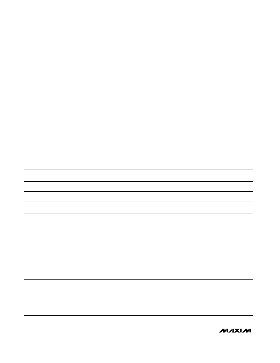
Bit 7
Bit 6
Bit 5
Bit 4
Bit 3
Bit 2
Bit 1
Bit 0
(MSB)
(LSB)
START
SEL2
SEL1
SEL0
UNI/
BIP
SGL/
DIF
PD1
PD0
Bit
Name
Description
7(MSB)
START
The first logic “
1
” bit after
CS goes low defines the beginning of the control byte.
6
SEL2
These three bits select which of the eight channels are used for the conversion.
5
SEL1
See Tables 3 and 4.
4
SEL0
3
UNI/
BIP
1
= unipolar,
0
= bipolar. Selects unipolar or bipolar conversion mode. In unipolar
mode, an analog input signal from 0V to VREF can be converted; in bipolar mode, the
signal can range from -VREF/2 to +VREF/2.
2
SGL/
DIF
1
= single ended,
0
= differential. Selects single-ended or differential conversions. In
single-ended mode, input signal voltages are referred to AGND. In differential mode,
the voltage difference between two channels is measured. See Tables 3 and 4.
1
PD1
Selects clock and power-down modes.
0(LSB)
PD0
PD1
PD0
Mode
0
0
Full power-down (I
Q
= 2µA)
0
1
Fast power-down (I
Q
= 30µA)
1
0
Internal clock mode
1 1
External clock mode
Table 2. Control-Byte Format