Detailed description – Rainbow Electronics MAX1143 User Manual
Page 9
MAX1142/MAX1143
14-Bit ADC, 200ksps, +5V Single-Supply
with Reference
_______________________________________________________________________________________
9
Detailed Description
The MAX1142/MAX1143 analog-to-digital converters
(ADCs) use a successive-approximation technique and
input track/hold (T/H) circuitry to convert an analog signal
to a 14-bit digital output. The MAX1142/MAX1143 easily
interfaces to microprocessors (µPs). The data bits can be
read either during the conversion in external clock mode
or after the conversion in internal clock mode.
In addition to a 14-bit ADC, the MAX1142/MAX1143
include an input scaler, an internal digital microcontroller,
calibration circuitry, an internal clock generator, and an
internal bandgap reference. The input scaler for the
MAX1142 enables conversion of input signals ranging
from 0 to +12V (unipolar input) or ±12V (bipolar input).
The MAX1143 accepts 0 to +4.096V (unipolar input) or
±4.096V (bipolar input). Input range selection is software
controlled.
Calibration
To minimize linearity, offset, and gain errors, the
MAX1142/MAX1143 have on-demand software calibra-
tion. Initiate calibration by writing a Control-Byte with bit
M1 = 0, and bit M0 = 1 (See Table 1). Select internal or
external clock for calibration by setting the INT/
EXT bit in
the Control-Byte. Calibrate the MAX1142/MAX1143 with
the clock used for performing conversions.
Offsets resulting from synchronous noise (such as the
conversion clock) are canceled by the MAX1142/
MAX1143’s calibration circuitry. However, because the
magnitude of the offset produced by a synchronous sig-
nal depends on the signal’s shape, recalibration may be
appropriate if the shape or relative timing of the clock or
other digital signals change, as might occur if more than
one clock signal or frequency is used.
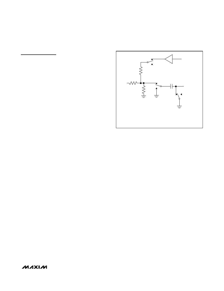
Input Scaler
The MAX1142/MAX1143 have an input scaler which
allows conversion of true bipolar input voltages while
operating from a single +5V supply. The input scaler
attenuates and shifts the input, as necessary, to map the
external input range to the input range of the internal
DAC. The MAX1142 analog input range is 0 to +12V
(unipolar) or ±12V (bipolar). The MAX1143 analog input
range is 0 to +4.096V (unipolar) or ±4.096V (bipolar).
Unipolar and bipolar mode selection is configured with bit
6 of the serial Control-Byte.
Figure 1 shows the equivalent input circuit of the
MAX1142/MAX1143. The resistor network on the analog
input provides ±16.5V fault protection. This circuit limits
the current going into or out of the pin, to less than 2mA.
The overvoltage protection is active, even if the device is
in a power-down mode, or if AV
DD
= 0.
Digital Interface
The digital interface pins consist of
SHDN, RST, SSTRB,
DOUT, SCLK, DIN and
CS. Bringing SHDN low, places
the MAX1142/MAX1143 in its 2.5µA shutdown mode. A
logic low on
RST halts the MAX1142/MAX1143 opera-
tion and returns the part to its power-on reset state.
In external clock mode, SSTRB is low and pulses high
for one clock cycle at the start of conversion. In internal
clock mode SSTRB goes low at the start of the conver-
sion, and goes high to indicate the conversion is fin-
ished.
The DIN input accepts Control-Byte data which is
clocked in on each rising edge of SCLK. After
CS goes
low or after a conversion or calibration completes, the
first logic “1” clocked-into DIN is interpreted as the
START bit, the MSB of the 8-bit Control-Byte.
The SCLK input is the serial data transfer clock which
clocks data in and out of the MAX1142/MAX1143.
SCLK also drives the A/D conversion steps in external
clock mode (see
Internal and External Clock Modes
section).
DOUT is the serial output of the conversion result.
DOUT is updated on the falling edge of SCLK. DOUT is
high-impedance when
CS is high.
CS must be low for the MAX1142/MAX1143 to accept a
Control-Byte. The serial interface is disabled when
CS
is high.
S1 = BIPOLAR/UNIPOLAR
S2, S3 = T/H SWITCH
S3
S2
AIN
S1
R1
2.5k
Ω
R3
R2
VOLTAGE
REFERENCE
T/H OUT
HOLD
HOLD
TRACK
TRACK
BIPOLAR
UNIPOLAR
R2 = 7.6k
Ω
(MAX1142)
OR 2.5k
Ω
(MAX1143)
R3 = 3.9k
Ω
(MAX1142)
OR INFINITY (MAX1143)
C
HOLD
30pF
Figure 1. Equivalent Input Circuit