Timing characteristics (figures 5 and 6) – Rainbow Electronics MAX1143 User Manual
Page 5
MAX1142/MAX1143
14-Bit ADC, 200ksps, +5V Single-Supply
with Reference
_______________________________________________________________________________________
5
Note 1:
Tested at AV
DD
= DV
DD
= +5V, bipolar input mode.
Note 2:
Relative accuracy is the deviation of the analog value at any code from its theoretical value after the gain error and offset
error have been nulled.
Note 3:
Offset nulled.
Note 4:
Conversion time is defined as the number of clock cycles multiplied by the clock period, clock has 50% duty cycle.
Includes the acquisition time.
Note 5:
ADC performance is limited by the converter’s noise floor, typically 300µVp-p.
Note 6
When an external reference has a different voltage than the specified typical value, the full scale of the ADC will scale
proportionally.
Note 7:
Electrical characteristics are guaranteed from AV
DD(MIN)
= DV
DD(MIN)
to AV
DD(MAX)
= DV
DD(MAX)
. For operations beyond
this range, see the
Typical Operating Characteristics
. For guaranteed specifications beyond the limits, contact
the factory.
Note 8:
Defined as the change in positive full-scale caused by a ±5% variation in the nominal supply voltage.
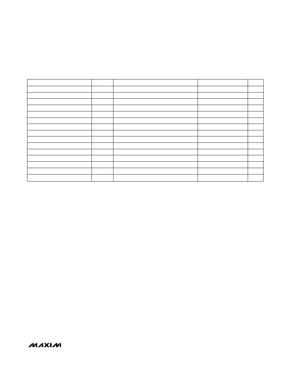
TIMING CHARACTERISTICS (Figures 5 and 6)
(AV
DD
= DV
DD
= +5V ±5%, T
A
= T
MIN
to T
MAX
, unless otherwise noted.)
PARAMETER
SYMBOL
CONDITIONS
MIN
TYP
MAX
UNIT
Acquisition Time
t
ACQ
1.14
µ
s
DIN to SCLK Setup
t
DS
50
ns
DIN to SCLK Hold
t
DH
0
ns
SCLK to DOUT Valid
t
DO
70
ns
CS Fall to DOUT Enable
t
DV
C
LOAD
= 50pF
80
ns
CS Rise to DOUT Disable
t
TR
C
LOAD
= 50pF
80
ns
CS to SCLK Rise Setup
t
CSS
100
ns
CS to SCLK Rise Hold
t
CSH
0
ns
SCLK High Pulse Width
t
CH
80
ns
SCLK Low Pulse Width
t
CL
80
ns
SCLK Fall to SSTRB
t
SSTRB
C
LOAD
= 50pF
80
ns
CS Fall to SSTRB Enable
t
SDV
C
LOAD
= 50pF, External clock mode
80
ns
CS Rise to SSTRB Disable
t
STR
C
LOAD
= 50pF, External clock mode
80
ns
SSTRB Rise to SCLK Rise
t
SCK
Internal clock mode
0
ns
RST Pulse Width
t
RS
208
ns