Applications information – Rainbow Electronics MAX1143 User Manual
Page 13
MAX1142/MAX1143
14-Bit ADC, 200ksps, +5V Single-Supply
with Reference
______________________________________________________________________________________
13
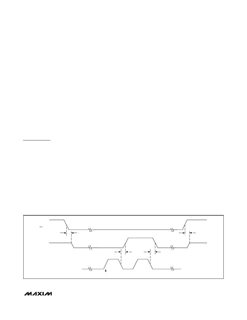
Data Framing
The falling edge of
CS does NOT start a conversion on
the MAX1142/MAX1143. The first logic high clocked
into DIN is interpreted as a start bit and defines the first
bit of the Control-Byte. A conversion starts on the falling
edge of SCLK, after the seventh bit of the Control-Byte
(the P1 bit) is clocked into DIN. The start bit is defined
as:
The first high bit clocked into DIN with
CS low, any-
time the converter is idle, e.g. after AV
DD
is applied,
or as the first high bit clocked into DIN after
CS is
pulsed high, then low.
OR
If a falling edge on
CS forces a start bit before the
conversion or calibration is complete, then the cur-
rent operation will be terminated and a new one
started.
Applications Information
Power-On Reset
When power is first applied to the MAX1142/MAX1143
or if
RST is pulsed low, the internal calibration registers
are set to their default values. The user-programmable
registers (P0, P1 and P2) are low, and the device is
configured for bipolar mode with internal clocking.
Calibration
To compensate the MAX1142/MAX1143 for tempera-
ture drift and other variations, they should be periodi-
cally calibrated. After any change in ambient
temperature more than 10°C, the device should be
recalibrated. A 100mV change in supply voltage or any
change in the reference voltage should be followed by
a calibration. Calibration corrects for errors in gain, off-
set, integral nonlinearity and differential nonlinearity.
The MAX1142/MAX1143 should be calibrated after
power-up or the assertion of reset. Make sure the
power supplies and the reference voltage have fully
settled prior to initiating the calibration sequence.
Initiate calibration by setting M1 = 0 and M0 = 1 in the
Control-Byte. In internal clock mode, SSTRB goes low
at the beginning of calibration and goes high to signal
the end of calibration, approximately 80,000 clock
cycles later. In external clock mode, SSTRB goes high
at the beginning of calibration and goes low to signal
the end of calibration. Calibration should be performed
in the same clock mode as will be used for conversions
(Figure 6).
Reference
The MAX1142/MAX1143 can be used with an internal or
external reference. An external reference can be con-
nected directly at the REF pin or at the REFADJ pin.
CREF is an internal reference node and must be
bypassed with a 1µF capacitor when using either the
internal or an external reference.
Internal Reference
When using the MAX1142/MAX1143’s internal refer-
ence, place a 0.22µF ceramic capacitor from REFADJ
to AGND and place a 2.2µF capacitor from REF to
AGND. Fine adjustments can be made to the internal
reference voltage by sinking or sourcing current at
REFADJ. The input impedance of REFADJ is nominally
9k
Ω
. The internal reference voltage is adjustable to
±1.5% with the circuit of Figure 7.
t
SDV
t
SSTRB
t
SSTRB
t
STR
P1 CLOCKED IN
SSTRB
SCLK
CS
Figure 6. External Clock Mode SSTRB Detailed Timing