Table 3. unipolar full scale and zero scale – Rainbow Electronics MAX1143 User Manual
Page 14
MAX1142/MAX1143
14-Bit ADC, 200ksps, +5V Single-Supply
with Reference
14
______________________________________________________________________________________
External reference
An external reference can be placed at either the input
(REFADJ) or the output (REF) of the MAX1142/
MAX1143’s internal buffer amplifier.
When connecting an external reference to REFADJ, the
input impedance is typically 9k
Ω
. Using the buffered
REFADJ input makes buffering of the external reference
unnecessary. The internal buffer output must be
bypassed at REF with a 2.2µF capacitor.
When connecting an external reference at REF,
REFADJ must be connected to AV
DD
. The input imped-
ance at REF is 16k
Ω
for DC currents. During conver-
sion, an external reference at REF must deliver 250µA
DC load current and have an output impedance of 10
Ω
or less. If the reference has a higher output impedance
or is noisy, bypass it at the REF pin with a 4.7µF capac-
itor.
Analog Input
The MAX1142/MAX1143 use a capacitive DAC that
provides an inherent track/hold function. Drive AIN with
a source impedance less than 10
Ω
. Any signal condi-
tioning circuitry must settle with 16-bit accuracy in less
than 500ns. Limit the input bandwidth to less than half
the sampling frequency to eliminate aliasing. The
MAX1142/MAX1143 has a complex input impedance
which varies from unipolar to bipolar mode (Figure 1).
Input Range
The analog input range in unipolar mode is 0 to +12V
for the MAX1142, and 0 to +4.096V for the MAX1143. In
bipolar mode, the analog input can be -12V to +12V for
the MAX1142, and -4.096V to +4.096V for the
MAX1143. Unipolar and bipolar mode is programmed
with the UNI/
BIP bit of the Control-Byte. When using a
reference other than the MAX1142/MAX1143’s internal
+4.096V reference, the full-scale input range will vary
accordingly. The full-scale input range depends on the
voltage at REF and the sampling mode selected (Tables
3 and 4).
Input Acquisition and Settling
Clocking-in a Control-Byte starts input acquisition. In
bipolar mode, the main capacitor array starts acquiring
the input as soon as a start bit is recognized. If unipolar
mode is selected by the second DIN bit, the part will
immediately switch to unipolar sampling mode and
acquire a sample.
Acquisition can be extended by eight clock cycles by
setting M1 = 1, M0 = 1 (long acquisition mode). The
sampling instant in short acquisition completes on the
falling edge of the sixth clock cycle after the start bit
(Figure 2).
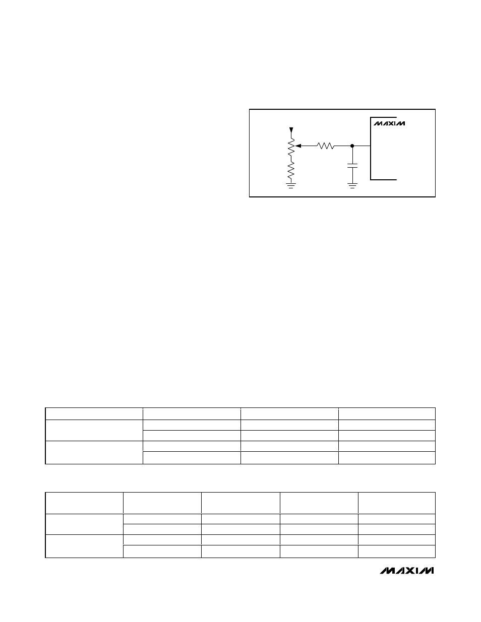
+5V
510k
Ω
100k
Ω
24k
Ω
0.22
µ
F
REFADJ
MAX1142
Figure 7. MAX1142 Reference-Adjust Circuit
Table 3. Unipolar Full Scale and Zero Scale
PART
REFERENCE
ZERO SCALE
FULL SCALE
Internal
0
+12V
MAX1142
External
0
+12(V
REF
/4.096)
Internal
0
+4.096V
MAX1143
External
0
+V
REF
Table 4. Bipolar Full Scale, Zero Scale, and Negative Scale
PART
REFERENCE
NEGATIVE FULL
SCALE
ZERO SCALE
FULL SCALE
Internal
-12V
0
+12V
MAX1142
External
-12(V
REF
/4.096)
0
+12(V
REF
/4.096)
Internal
-4.096V
0
+4.096V
MAX1143
External
-V
REF
0
+V
REF