Rainbow Electronics MAX1143 User Manual
Page 15
MAX1142/MAX1143
14-Bit ADC, 200ksps, +5V Single-Supply
with Reference
______________________________________________________________________________________
15
Acquisition is 5.5 clock cycles in short acquisition
mode and 13.5 clock cycles in long acquisition mode.
Short acquisition mode is 24 clock cycles per conver-
sion. Using the external clock to run the conversion
process limits unipolar conversion speed to 125ksps
instead of 200ksps in bipolar mode. The input resis-
tance in unipolar mode is larger than that of bipolar
mode (Figure1). The RC time constant in unipolar mode
is larger than that of bipolar mode, reducing the maxi-
mum conversion rate in 24 external clock mode. Long
acquisition mode with external clock allows both unipo-
lar and bipolar sampling of 150ksps (4.8MHz/32 clock
cycles) by adding eight extra clock cycles to the con-
version.
Most applications require an input buffer amplifier. If
the input signal is multiplexed, the input channel should
be switched immediately after acquision, rather than
near the end of or after a conversion. This allows more
time for the input buffer amplifier to respond to a large
step change in input signal. The input amplifier must
have a high enough slew-rate to complete the required
output voltage change before the beginning of the
acquisition time. At the beginning of acquisition, the
capacitive DAC is connected to the amplifier output,
causing some output disturbance. Ensure that the sam-
pled voltage has settled to within the required limits
before the end of the acquisition time. If the frequency
of interest is low, AIN can be bypassed with a large
enough capacitor to charge the capacitive DAC with
very little change in voltage. However, for AC use, AIN
must be driven by a wideband buffer (at least 10MHz),
which must be stable with the DAC’s capacitive load (in
parallel with any AIN bypass capacitor used) and also
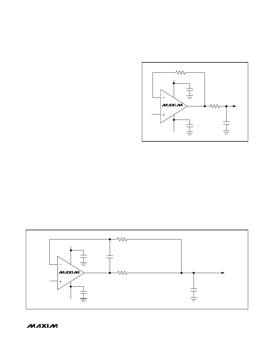
settle quickly (Figures 8 or 9).
Digital Noise
Digital noise can couple to AIN and REF. The conver-
sion clock (SCLK) and other digital signals that are
active during input acquisition, contribute noise to the
conversion result. If the noise signal is synchronous to
the sampling interval, an effective input offset is pro-
duced. Asynchronous signals produce random noise
on the input, whose high-frequency components may
be aliased into the frequency band of interest. Minimize
noise by presenting a low impedance (at the frequen-
cies contained in the noise signal) at the inputs. This
requires bypassing AIN to AGND, or buffering the input
with an amplifier that has a small-signal bandwidth of
several MHz, or preferably both. AIN has a bandwidth
of about 4MHz.
4
7
6
2
3
IN
+15V
-15V
0.0033
µ
F
0.1
µ
F
0.1
µ
F
1k
Ω
20
Ω
AIN
MAX427
1000pF
Figure 8. AIN Buffer for AC/DC Use
4
7
6
2
3
IN
+5V
-5V
AIN
0.1
µ
F
0.1
µ
F
0.1
µ
F
22
Ω
510
Ω
MAX410
Figure 9. ±5V Buffer for AC/DC Use has ±3.5V Swing