Table 2. user-programmable outputs, Output data – Rainbow Electronics MAX1143 User Manual
Page 11
MAX1142/MAX1143
14-Bit ADC, 200ksps, +5V Single-Supply
with Reference
______________________________________________________________________________________
11
In external clock mode, SSTRB is high-impedance
when
CS is high. In external clock mode, CS is normally
held low during the entire conversion. If
CS goes high
during the conversion, SCLK is ignored until
CS goes
low. This allows external clock mode to be used with 8-
bit bytes.
Internal Clock
In internal clock mode, the MAX1142/MAX1143 gener-
ates its own conversion clock. This frees the micro-
processor from the burden of running the SAR conver-
sion clock, and allows the conversion results to be read
back at the processor’s convenience, at any clock rate
up to 8MHz.
SSTRB goes low at the start of the conversion and goes
high when the conversion is complete. SSTRB will be
low for a maximum of 6µs, during which time SCLK
should remain low for best noise performance. An inter-
nal register stores data when the conversion is in
progress. SCLK clocks the data out of the internal stor-
age register at any time after the conversion is com-
plete.
The MSB of the conversion is available at DOUT when
SSTRB goes high. The subsequent 15 falling edges on
SCLK shift the remaining bits out of the internal storage
register (Figure 4).
CS does not need to be held low
once a conversion is started.
When internal clock mode is selected, SSTRB does not
go into a high-impedance state when
CS goes high.
Figure 5 shows the SSTRB timing in internal clock
mode. In internal clock mode, data can be shifted into
the MAX1142/MAX1143 at clock rates up to 4.8MHz,
provided that the minimum acquisition time,
t
ACQ
, is kept above 1.14µs in bipolar mode and 1.82µs
in unipolar-mode. Data can be clocked out at 8MHz.
Output Data
The output data format is straight binary for unipolar
conversions and two’s complement in bipolar mode. In
both modes the MSB is shifted out of the MAX1142/
MAX1143 first.
Table 2. User-Programmable Outputs
OUTPUT
PIN
PROGRAMMED
THROUGH
CONTROL-
BYTE
POWER-ON
OR
RST
DEFAULT
DESCRIPTION
P2
Bit 2
0
P1
Bit 1
0
P0
Bit 0
0
U ser p r og r am m ab l e outp uts fol l ow the state of the C ontr ol - Byte’ s thr ee LS Bs,
and ar e up d ated si m ul taneousl y w hen a new C ontr ol - Byte i s w r i tten. O utp uts
ar e p ush- p ul l . In har d w ar e and softw ar e shutd ow n, these outp uts ar e
unchang ed and r em ai n l ow - i m p ed ance.
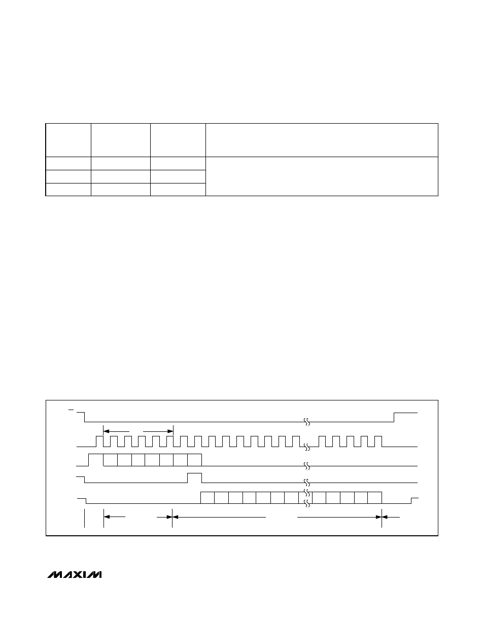
ACQUISITION
CONVERSION
IDLE
IDLE
SCLK
DOUT
A/D
STATE
DIN
SSTRB
CS
4
1
8
12
START
M1
M0
P2
P1
P0
UNI/
BIP
INT/
EXT
15
21
24
B10
B9
B12
B11
B8
B7
B2
B13
MSB
B0
LSB
FILLED WITH
ZEROS
B1
X
X
t
ACQ
Figure 2. Short Acquisition Mode (24-Clock Cycles) External Clock, Bipolar Mode