Table 1. control-byte format – Rainbow Electronics MAX1143 User Manual
Page 10
MAX1142/MAX1143
14-Bit ADC, 200ksps, +5V Single-Supply
with Reference
10
______________________________________________________________________________________
User-Programmable Outputs
The MAX1142/MAX1143 have three user-programma-
ble outputs: P0, P1 and P2. The power-on default state
for the programmable outputs is zero. These are push-
pull CMOS outputs suitable for driving a multiplexer, a
PGA, or other signal preconditioning circuitry. The user-
programmable outputs are controlled by bits 0, 1 and 2
of the Control-Byte (Table 2).
The user-programmable outputs are set to zero during
power-on reset (POR) or when
RST goes low. During
hardware or software shutdown P0, P1, and P2 are
unchanged and remain low-impedance.
Starting a Conversion
Start a conversion by clocking a Control-Byte into the
device’s internal shift register. With
CS low, each rising
edge on SCLK clocks a bit from DIN into the
MAX1142/MAX1143’s internal shift register. After
CS
goes low or after a conversion or calibration completes,
the first arriving logic “1” is defined as the start bit of
the Control-Byte. Until this first start bit arrives, any
number of logic “0” bits can be clocked into DIN with
no effect. If at any time during acquisition or conversion,
CS is brought high and then low again, the part is
placed into a state where it can recognize a new start
bit. If a new start bit occurs before the current conver-
sion is complete, the conversion is aborted and a new
acquisition is initiated. Table 1 shows the Control-Byte
format.
Internal and External Clock Modes
The MAX1142/MAX1143 may use either the external
serial clock or the internal clock to perform the succes-
sive-approximation conversion. In both clock modes,
the external clock shifts data in and out of the
MAX1142/MAX1143. Bit 5 (INT/
EXT) of the Control-Byte
programs the clock mode.
External Clock
In external clock mode, the external clock not only
shifts data in and out, but it also drives the A/D conver-
sion steps. In short acquisition mode, SSTRB pulses
high for one clock period after the seventh falling edge
of SCLK, following the start bit. The MSB of the conver-
sion is available at DOUT on the eighth falling edge of
SCLK (Figure 2).
In long acquisition mode, when using the external
clock, SSTRB pulses high for one clock period after the
fifteenth falling edge of SCLK, following the start bit.
The MSB of the conversion is available at DOUT on the
sixteenth falling edge of SCLK (Figure 3).
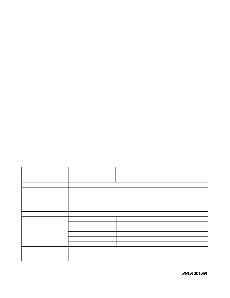
Table 1. Control-Byte Format
BIT7
(MSB)
BIT6
BIT5
BIT4
BIT3
BIT2
BIT1
BIT0
(LSB)
START
UNI/
BIP
INT/
EXT
M1
M0
P2
P1
P0
BIT
NAME
DESCRIPTION
7 (MSB)
START
The first logic “1” bit, after
CS goes low, defines the beginning of the Control-Byte
6
UNI/
BIP
1 = unipolar, 0 = bipolar. Selects unipolar or bipolar conversion mode. In unipolar mode, analog
input signals from 0 to +12V (MAX1142) or 0 to V
REF
(MAX1143) can be converted. In bipolar
mode analog input signals from -12V to +12V (MAX1142) or -V
REF
to +V
REF
(MAX1143) can be
converted.
5
INT/
EXT
Selects the internal or external conversion clock. 1 = Internal, 0 = External.
4
M1
M1
M0
MODE
0
0
24 External clocks per conversion (short acquisition mode)
0
1
Start Calibration. Starts internal calibration
1
0
Software power-down mode
3
M0
1
1
32 External clocks per conversion (long acquisition mode)
2
1
0(LSB)
P2
P1
P0
These three bits are stored in a port register and output to pins P2–P0 for use in addressing a
MUX or PGA. These three bits are updated in the port register simultaneously when a new
Control-Byte is written.