Absolute maximum ratings, Electrical characteristics – Rainbow Electronics MAX1143 User Manual
Page 2
MAX1142/MAX1143
14-Bit ADC, 200ksps, +5V Single-Supply
with Reference
2
_______________________________________________________________________________________
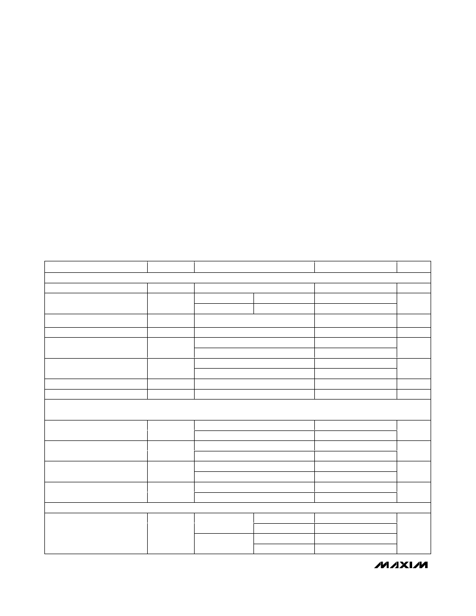
ABSOLUTE MAXIMUM RATINGS
Stresses beyond those listed under “Absolute Maximum Ratings” may cause permanent damage to the device. These are stress ratings only, and functional
operation of the device at these or any other conditions beyond those indicated in the operational sections of the specifications is not implied. Exposure to
absolute maximum rating conditions for extended periods may affect device reliability.
AV
DD
to AGND, DV
DD
to DGND .............................-0.3V to +6V
AGND to DGND.....................................................-0.3V to +0.3V
AIN to AGND.....................................................................±16.5V
REFADJ, CREF, REF to AGND.................-0.3V to (AV
DD
+ 0.3V)
Digital Inputs to DGND.............................................-0.3V to +6V
Digital Outputs to DGND .........................-0.3V to (DV
DD
+ 0.3V)
Continuous Power Dissipation (T
A
= +70°C)
20-SSOP (derate 8.00mW/°C above +70°C) ...............640mW
Operating Temperature Ranges
MAX114_CAP ......................................................0°C to +70°C
MAX114_EAP....................................................-40°C to +85°C
Storage Temperature Range .............................-60°C to +150°C
Junction Temperature ......................................................+150°C
Lead Temperature (soldering, 10s) .................................+300°C
ELECTRICAL CHARACTERISTICS
(AV
DD
= DV
DD
= +5V ±5%, f
SCLK
= 4.8MHz, external clock (50% duty cycle), 24 clocks/conversion (200ksps), bipolar input, external
V
REF
= +4.096V, V
REFADJ
= AV
DD
, C
REF
= 2.2µF, C
CREF
= 1µF, T
A
= T
MIN
to T
MAX
, unless otherwise noted. Typical values are at
T
A
= +25°C.)
PARAMETER
SYMBOL
CONDITIONS
MIN
TYP
MAX
UNITS
DC ACCURACY
(Note 1)
Resolution
14
Bits
Unipolar Mode
MAX114_A
±
1
Relative Accuracy (Note 2)
INL
MAX114_B
±
2
LSB
Differential Nonlinearity
DNL
Unipolar Mode
±
1
LSB
Transition Noise
0.34
LSB RMS
Unipolar
±
4
Offset Error
Bipolar
±
6
mV
Unipolar
±
0.2
Gain Error (Note 3)
Bipolar
±
0.3
%FSR
Offset D r i ft ( Bi p ol ar and U ni p ol ar )
Excluding reference drift
±
1
ppm/
o
C
G ai n D r i ft ( Bi p ol ar and U ni p ol ar )
Excluding reference drift
±
1
ppm/
o
C
DYNAMIC SPECIFICATIONS
(5kHz sine-wave input, 200ksps, 4.8MHz clock, bipolar input mode).
(MAX1142, 24Vp-p. MAX1143, 8.192Vp-p)
f
IN
= 5kHz
81
SINAD
f
IN
= 100kHz
82
dB
f
IN
= 5kHz
82
SNR
f
IN
= 100kHz
82
dB
f
IN
= 5kHz
-88
THD
f
IN
= 100kHz
91
dB
f
IN
= 5kHz
90
SFDR
f
IN
= 100kHz
95
dB
ANALOG INPUT
Unipolar
0
12
MAX1142
Bipolar
-12
12
Unipolar
0
4.096
Input Range
MAX1143
Bipolar
- 4.096
4.096
V