Isd5100 – series, Isd5102, Isd5102 device – Rainbow Electronics ISD5100 User Manual
Page 84
ISD5100 – SERIES
- 84 -
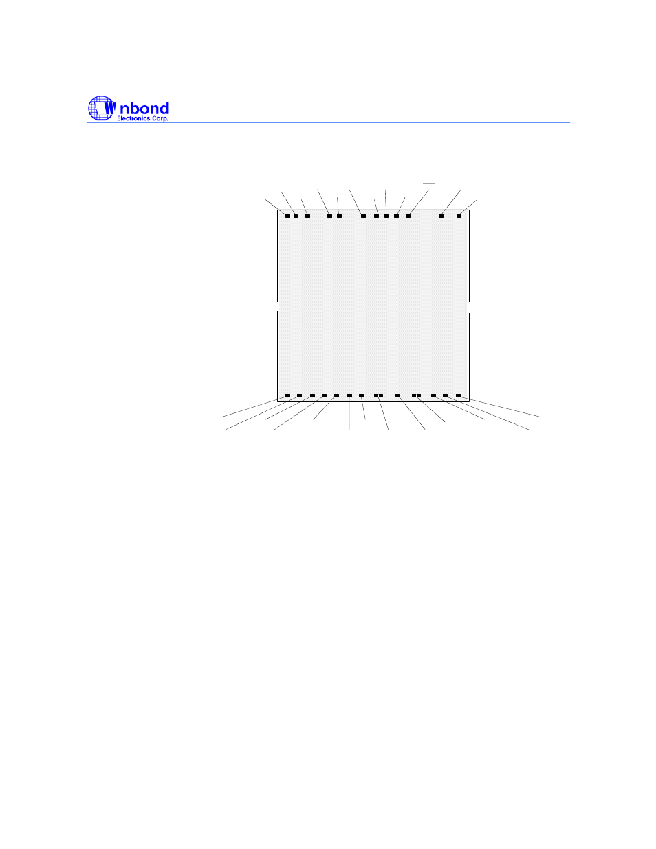
12.7 ISD5102 D
IE
I
NFORMATION
≈
ISD5102
≈
V
SSA
MIC +
MIC -
ANA OUT +
ANA OUT -
ACAP
SP -
V
SSA
[2]
SP +
V
CCA
[2]
ANA IN
AUX IN
AUX OUT
V
SSD
V
SSD
A0
SDA
A1
SCL
V
CCD
XCLK
RAC
V
SSA
INT
V
CCD
ISD5102 Device
Die Dimensions (include scribe line)
X: 4230 µm
Y: 5046 µm
Die Thickness
[3]
292.1 µm ± 12.7 µm
Pad Opening
Single pad: 90 x 90 µm
Double pad: 180 x 90 µm
Notes
1.
The backside of die is internally connected to Vss. It MUST NOT be connected to any other potential or
damage may occur.
2.
Double bond recommended, if treated as single doubled-pad.
3.
This figure reflects the current die thickness. Please contact Winbond as this thickness may change in
the future.