Isd5100 – series – Rainbow Electronics ISD5100 User Manual
Page 55
ISD5100 – SERIES
Publication Release Date: October, 2003
- 55 -
Revision 0.2
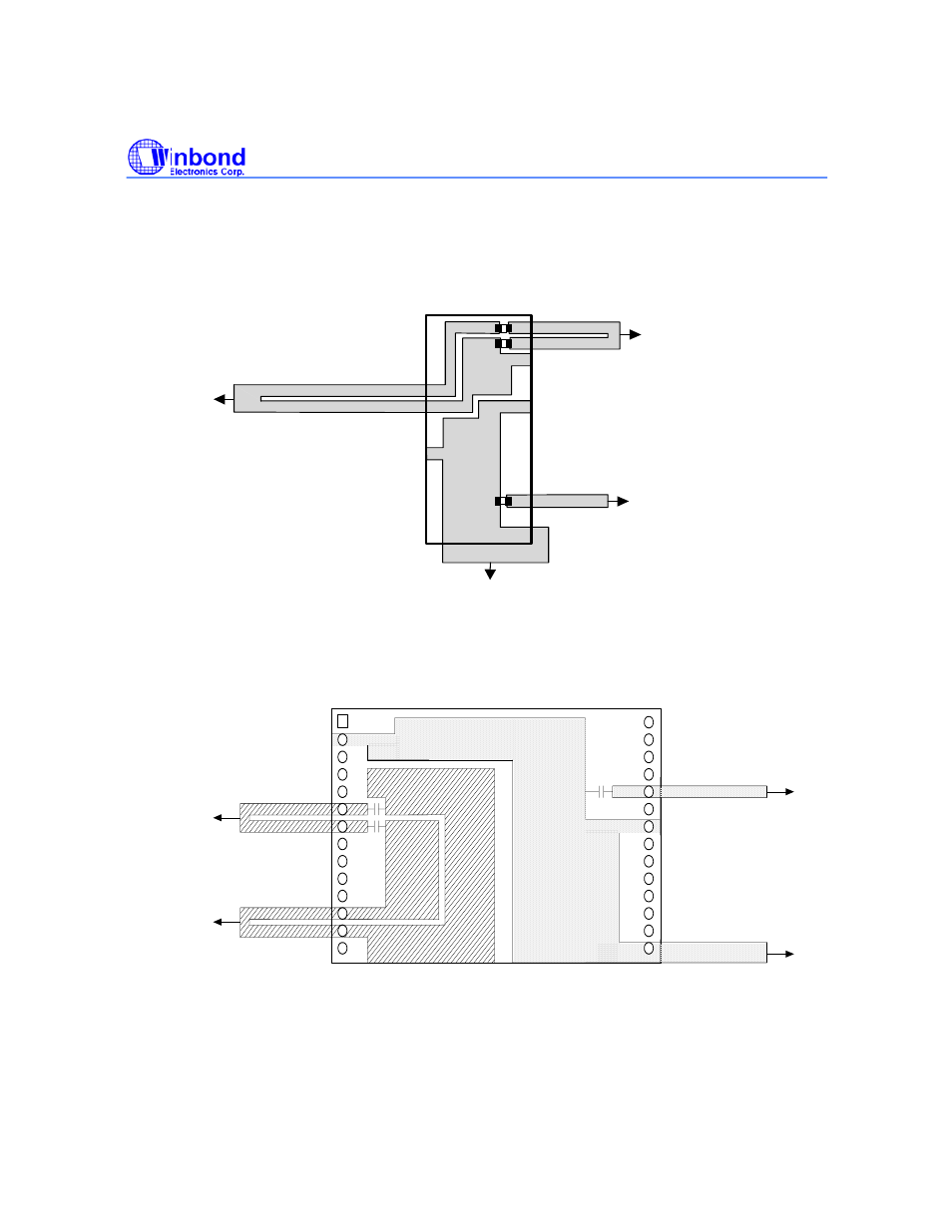
7.6.4. PCB Layout Examples
For SOIC package :
PC board traces and the three chip capacitors are on the bottom side of the board.
O
O
O
O
O
O
O
O
O
O
O
O
O
O
O
O
O
O
O
O
O
O
O
O
O
O
O
O
V
C
C
D
XCLK
Analog Ground
1
V
SS A
To
V
CC A
V
S
S
D
(Digital Ground)
Note 1: V
SSD
traces should be kept
separated back to the V
SS
supply feed
point..
Note 2: V
CCD
traces should be kept
separate back to the V
CC
Supply feed
point.
Note 3: The Digital and Analog grounds
tie together at the power supply. The
V
CCA
and V
CCD
supplies will also need
filter capacitors per good engineering
practice (typ. 50 to 100 uF).
C1
C2
C3
Note 1
Note 2
C1=C2=C3=0.1 uF chip Capacitors
Note 3
Note 3
For TSOP package :
Notes:
[1]
V
SSD
traces should be kept separated back to the V
SS
supply feedpoint.
[2]
V
CCD
traces should be kept separate back to the V
CC
supply feedpoint.
[3]
Digital and Analog grounds tie together at power supply. The V
CCA
and V
CCD
supplies will also need filter
capacitors per good engineering practice (typ. 50 to 100 uF).
V
CCA
V
SSA
V
SSD
V
CCD
Note
[2]
Note
[1]
Note
[3]
V
CCD
V
CCD
V
SSD
V
SSD
V
SSA
V
SSA
V
CCA
V
SSA
1