Isd5100 – series, Pin description – Rainbow Electronics ISD5100 User Manual
Page 8
ISD5100 – SERIES
- 8 -
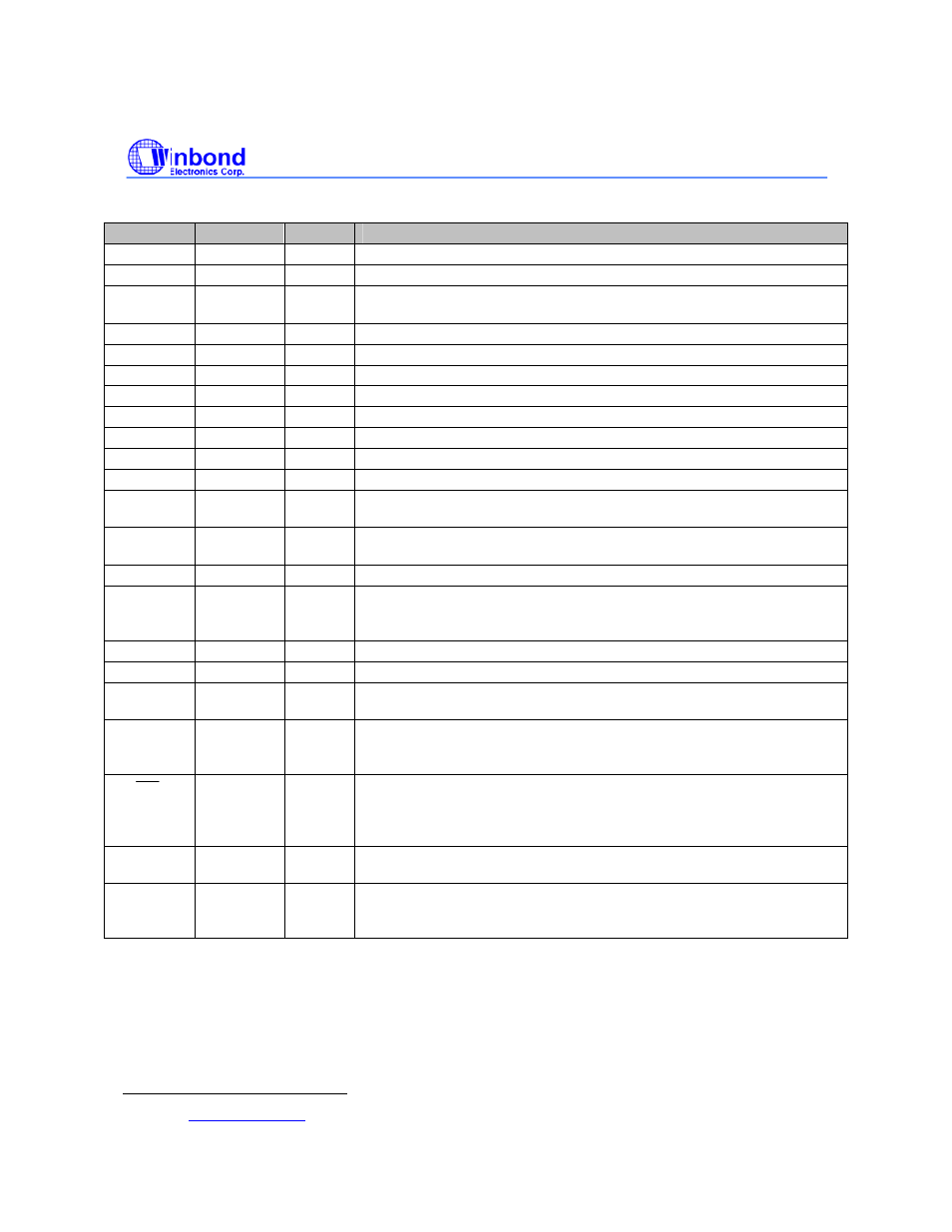
6. PIN DESCRIPTION
Pin Name
SOIC/PDIP TSOP
Functionality
SCL 1 8
I
2
C Serial Clock Line: to clock the data into and out of the I
2
C interface.
A1
2
9
Input pin that supplies the LSB +1 bit for the I
2
C Slave Address.
SDA 3 10
I
2
C Serial Data Line: Data is passed between devices on the bus over
this line.
A0
4
11
Input pin that supplies the LSB for the I
2
C Slave Address.
V
SSD
5,6 12,13
Digital
Ground.
NC 7,21,22
1,14,28
No
Connect.
MIC+
8
16
Differential Positive Input for the microphone amplifier.
V
SSA
9,15,23 2,15,22
Analog
Ground.
MIC-
10
17
Differential Negative Input for the microphone amplifier.
ANA OUT+
11
18
Differential Positive Analog Output for ANA OUT.
ANA OUT-
12
19
Differential Negative Analog Output for ANA OUT.
ACAP
13
20
AGC/AutoMute Capacitor: Required for the on-chip AGC amplifier during
record and AutoMute function during playback.
SP-
14
21
Differential Negative Speaker Output: When the speaker outputs are in
use, the AUX OUT output is disabled.
SP+
16
23
Differential Positive Speaker Output.
V
CCA
17
24
Analog Supply Voltage: This pin supplies power to the analog sections
of the device. It should be carefully bypassed to Analog Ground to
insure correct device operation.
ANA IN
18
25
Analog Input: one of the analog inputs with selectable gain.
AUX IN
19
26
Auxiliary Input: one of the analog inputs with selectable gain.
AUX OUT
20
27
Auxiliary Output: one the analog outputs of the device. When this
output is used, the SP+ and SP- outputs are disabled.
RAC
24
3
Row Address Clock; an open drain output. The RAC pin goes LOW
T
RACL
[1]
before the end of each row of memory and returns HIGH at
exactly the end of each row of memory.
INT
25
4
Interrupt Output; an open drain output that indicates that a set EOM bit
has been found during Playback or that the chip is in an Overflow (OVF)
condition. This pin remains LOW until a Read Status command is
executed.
XCLK
26
5
This pin allows the internal clock of the device to be driven externally for
enhanced timing precision. This pin is grounded for most applications.
V
CCD
27,28
6,7
Digital Supply Voltage. These pins supply power to the digital sections
of the device. They must be carefully bypassed to Digital Ground to
insure correct device operation.
[1]
See the
Parameters section