Video output, Pixel order, Synchronization: the dummy column – Rainbow Electronics AT77C101B FingerChip™ User Manual
Page 15
15
AT77C101B
2150A–BIOM–02/02
Video Output
An analog signal is also available on pins AVE and AVO. Note that video output is avail-
able one clock pulse before the corresponding digital output (one clock pipe-line delay
for the analog to digital conversion).
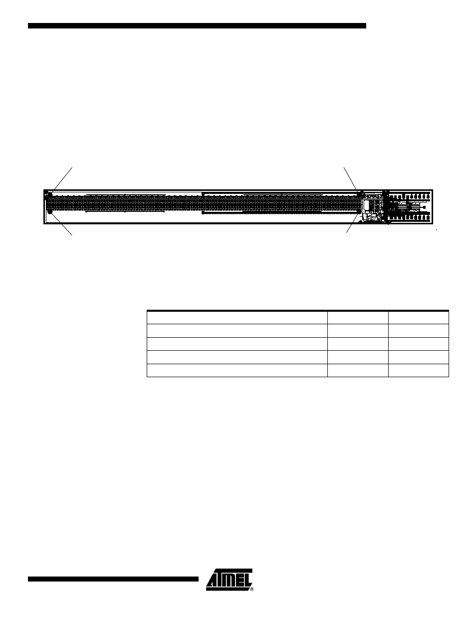
Pixel Order
After a reset, pixel number one is located on the upper left corner, looking at the chip
with bond pads to the right. For each column of 8 pixels, pixels 1-3-5-7 are output on
odd data Do0-3 pins, pixels 2-4-6-8 are output on even data De0-3 pins. Most significant
bit is bit #3, least significant is bit #0.
Figure 11. Pixel Order
Synchronization: The
Dummy Column
A dummy column has been added to the sensor to act as a specific pattern to detect the
first pixel. So, 280 true columns + 1 dummy column are read for each frame.
The 4 bytes of the dummy column contain a fixed pattern on the two first bytes, and tem-
perature information on the last two bytes.
Note:
x represents 0 or 1
The sequence 111X0000 111X0000 appears on every frame (exactly every 1124 clock
pulses), so it is an easy pattern to recognize for synchronization purposes.
B ond pads
Pixel #1 (1,1)
Pixel #2233 (280,1)
Pixel #8 (1,8)
Pixel #2240 (280,8)
Dummy Byte
Odd
Even
Dummy Byte 1 DB1:
111X
0000
Dummy Byte 2 DB2:
111X
0000
Dummy Byte 3 DB3:
rrrr
nnnn
Dummy Byte 4 DB4:
tttt
pppp