Pin configuration and function descriptions, Recommended layout – Rainbow Electronics DAB-IMU-C01 User Manual
Page 7
ADIS16250/ADIS16255
Rev. B | Page 7 of 20
PIN CONFIGURATION AND FUNCTION DESCRIPTIONS
DNC = DO NOT CONNECT
20
19
18
17
16
15
14
13
12
11
10
9
8
7
6
5
4
3
2
1
DNC
COM
DNC
DNC
DIO1 RST
VREF
COM VCC VCC
DNC
AUX
DAC
AUX
ADC
RATE
FILT
DIO0
CS
DIN
DOUT
SCLK
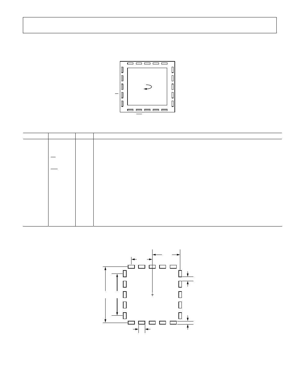
POSITIVE OUTPUT
ROTATIONAL
DIRECTION
TOP VIEW
(Not To Scale)
ADIS16250/
ADIS16255
06
070
-00
4
Figure 5. Pin Configuration
Table 4. Pin Function Descriptions
Pin No.
Mnemonic
Type
Description
1
SCLK
I
SPI, Serial Clock.
2
DOUT
O
SPI, Data Output.
3
DIN
I
SPI, Data Input.
4
CS
I
SPI, Chip Select, Active Low.
5, 6
DIO0, DIO1
I/O
Multifunction Digital Input/Output Pin.
7
RST
I
Reset, Active Low. This resets the sensor signal conditioning circuit and initiates a start-up sequence.
8, 9, 10, 11
DNC
–
Do Not Connect.
12
AUX DAC
O
Auxiliary DAC Analog Output Voltage.
13
AUX ADC
I
Auxiliary ADC Analog Input Voltage.
14
RATE
O
Analog Rate Signal Output (Uncalibrated).
15 FILT I
Analog Amplifier Summing Junction. This is used for setting the analog bandwidth. See the Analog
Bandwidth section for more details.
16, 17
VCC
S
5.0 V Power Supply.
18, 19
COM
S
Common. Reference point for all circuitry in the ADIS16250/ADIS16255.
20
VREF
O
Precision Reference Output.
1
S = supply; O = output; I = input.
RECOMMENDED LAYOUT
3.800
8Ч
5.0865
8Ч
0.773
16Ч
0.500
20Ч
1.127
20Ч
10.173
2Ч
7.600
4Ч
06
07
0-
01
0
11mm × 11mm STACKED LGA PACKAGE
Figure 6. Recommended Pad Layout (Units in Millimeters)