Timing specifications – Rainbow Electronics DAB-IMU-C01 User Manual
Page 5
ADIS16250/ADIS16255
Rev. B | Page 5 of 20
TIMING SPECIFICATIONS
T
A
= −40°C to +85°C, V
CC
= 5.0 V, unless otherwise noted.
Table 2.
Parameter Description
Min
Typ Max
Unit
f
SCLK
Fast mode, SMPL_PRD ≤ 0x07 (f
S
≥ 64 Hz)
0.01
2.5
MHz
Normal mode, SMPL_PRD ≥ 0x08 (f
S
≤ 56.9 Hz)
0.01
1.0
MHz
t
DATARATE
Data rate period, fast mode, SMPL_PRD ≤ 0x07 (f
S
≥ 64 Hz)
32
μs
Data rate period, normal mode, SMPL_PRD ≥ 0x08 (f
S
≤ 56.9 Hz)
42
μs
t
STALL
Stall period, fast mode, SMPL_PRD ≤ 0x07 (f
S
≥ 64 Hz)
9
μs
Stall period, normal mode, SMPL_PRD ≥ 0x08 (f
S
≤ 56.9 Hz)
12 μs
t
CS
Chip select to clock edge
48.8
ns
t
DAV
Data output valid after SCLK falling edge
100
ns
t
DSU
Data input setup time before SCLK rising edge
24.4
ns
t
DHD
Data input hold time after SCLK rising edge
48.8
ns
t
DF
Data output fall time
5
12.5
ns
t
DR
Data output rise time
5
12.5
ns
t
SFS
CS high after SCLK edge
5
ns
Flash update time (power supply must be within range)
50
ms
1
Guaranteed by design; not production tested.
2
The MSB presents an exception to this parameter. The MSB clocks out on the falling edge of CS. The rest of the DOUT bits are clocked after the falling edge of SCLK and
are governed by this specification.
3
This parameter may need to be expanded to allow for proper capture of the LSB. After CS goes high, the DOUT line goes into a high impedance state.
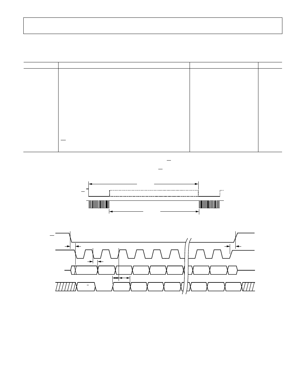
CS
SCLK
t
DATARATE
t
DATASTALL
060
70
-02
6
Figure 2. SPI Chip Select Timing
CS
SCLK
DOUT
DIN
1
2
3
4
5
6
15
16
W/R
A5
A4
A3
A2
D2
MSB
DB14
D1
LSB
DB13
DB12
DB10
DB11
DB2
LSB
DB1
t
CS
t
SFS
t
DAV
t
DHD
t
DSU
*
*NOT DEFINED
06
07
0-
0
03
Figure 3. SPI Timing
(Utilizing SPI Settings Typically Identified as Phase = 1, Polarity = 1)