Basic operation, Serial peripheral interface (spi), Writing to registers – Rainbow Electronics DAB-IMU-C01 User Manual
Page 11: Reading from registers
ADIS16250/ADIS16255
Rev. B | Page 11 of 20
BASIC OPERATION
The ADIS16250/ADIS16255 are designed for simple integration
into industrial system designs, requiring only a 5.0 V power
supply and a 4-wire, industry standard serial peripheral interface
(SPI). All outputs and user-programmable functions are
handled by a simple register structure. Each register is 16 bits in
length and has its own unique bit map. The 16 bits in each
register consist of an upper (D8 to D15) byte and a lower (D0 to
D7) byte, each of which has its own 6-bit address.
SERIAL PERIPHERAL INTERFACE (SPI)
The ADIS16250/ADIS16255 serial peripheral interface (SPI)
port includes four signals: chip select (CS), serial clock (SCLK),
data input (DIN), and data output (DOUT). The CS line
enables the ADIS16250/ADIS16255 SPI port and frames each
SPI event, which consists of single or multiple data frames.
When this signal is high, the DOUT lines are in a high
impedance state and the signals on DIN and SCLK have no
impact on operation. A complete data frame contains 16 clock
cycles. Because the SPI port operates in full duplex mode, it
supports simultaneous, 16-bit receive (DIN) and transmit
(DOUT) functions during the same data frame.
Table 2, Figure 2, and Figure 3 for detailed timing and
operation of the SPI port.
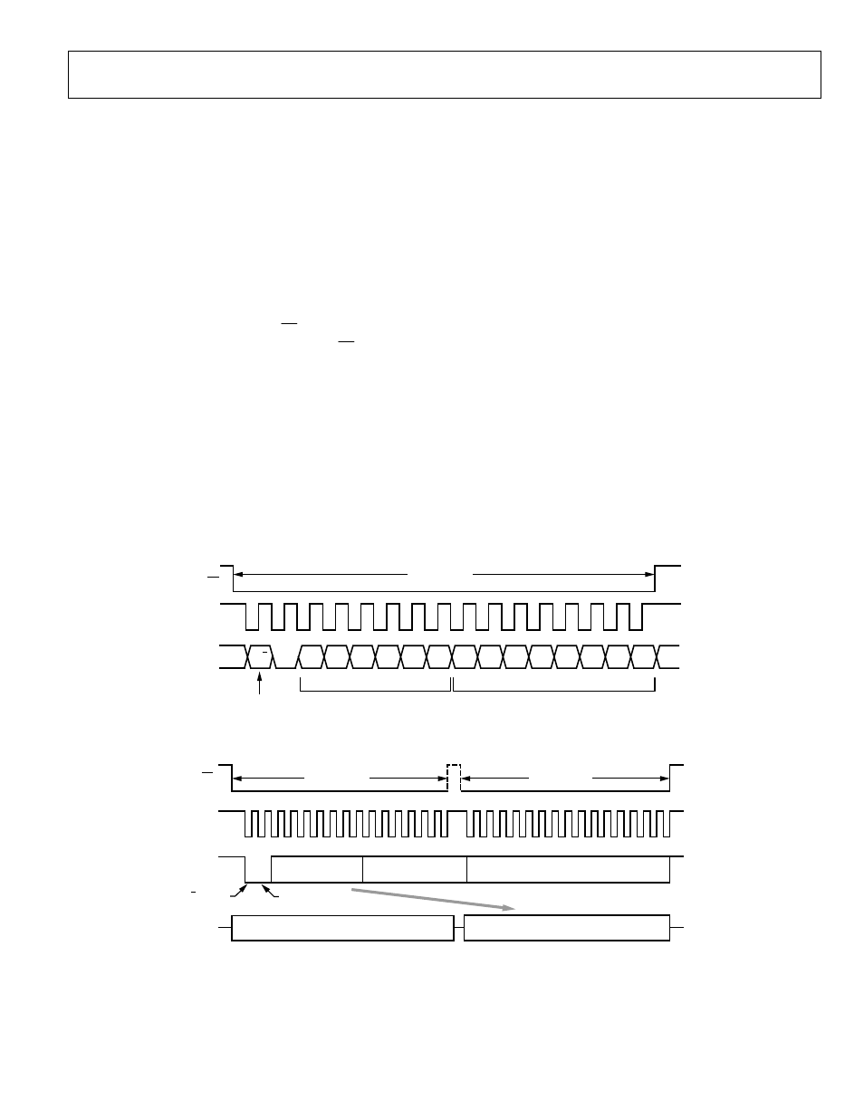
Writing to Registers
Figure 20 displays a typical data frame for writing a command
to a control register. In this case, the first bit of the DIN se-
quence is a 1, followed by a 0, the 6-bit address, and the 8-bit
data command. Because each write command covers a single
byte of data, two data frames are required when writing the entire
16-bit space of a register.
Reading from Registers
Reading the contents of a register requires a modification to the
sequence in Figure 20. In this case, the first two bits in the DIN
sequence are 0, followed by the address of the register. Each register
has two addresses (upper, lower), but either one can be used to
access its entire 16 bits of data. The final eight bits of the DIN
sequence are irrelevant and can be counted as don’t cares during a
read command. During the next data frame, the DOUT sequence
contains the register’s 16-bit data, as shown in Figure 21.
Although a single read command requires two separate data
frames, the full duplex mode minimizes this overhead, requiring
only one extra data frame when continuously sampling.
CS
SCLK
DIN
06
07
0-
0
06
W/R
A5
A4
A3
A2
A1
A0
DC7 DC6 DC5 DC4 DC3 DC2 DC1 DC0
DATA FRAME
WRITE = 1
READ = 0
REGISTER ADDRESS
DATA FOR WRITE COMMANDS
DON’T CARE FOR READ COMMANDS
Figure 20. DIN Bit Sequence
ADDRESS
DON’T CARE
NEXT COMMAND
BASED ON PREVIOUS COMMAND
DATA FRAME
16-BIT REGISTER CONTENTS
SCLK
DIN
DON’T
CARE
DON’T
CARE
DOUT
ZERO
CS
W/R BIT
DATA FRAME
06
07
0-
0
07
Figure 21. SPI Sequence for Read Commands