Ata6837 [preliminary, Functional description, 1 serial interface – Rainbow Electronics ATA6837 User Manual
Page 5
5
4953C–AUTO–09/07
ATA6837 [Preliminary]
3.
Functional Description
3.1
Serial Interface
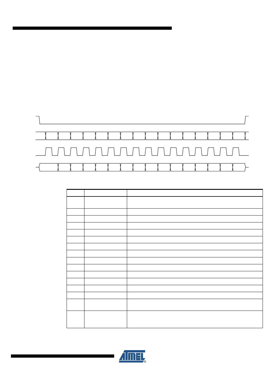
Data transfer starts with the falling edge of the CS signal. Data must appear at DI synchronized
to CLK and is accepted on the falling edge of the CLK signal. LSB (bit 0, SRR) has to be trans-
ferred first. Execution of new input data is enabled on the rising edge of the CS signal. When CS
is high, pin DO is in a tri-state condition. This output is enabled on the falling edge of CS. Output
data will change their state with the rising edge of CLK and stay stable until the next rising edge
of CLK appears. LSB (bit 0, TP) is transferred first.
Figure 3-1.
Data Transfer Input Data Protocol
SRR
LS1
HS1
LS2
HS2
LS3
HS3
LS4
HS4
LS5
HS5
LS6
HS6
OLD
SCT
SI
CS
DI
CLK
DO
TP
SLS1
SHS1
SLS2
SHS2
SLS3
SHS3
SLS4
SHS4
SLS5
SHS5
SLS6
SHS6
SCD
INH
PSF
0
1
2
3
4
5
6
7
8
9
10
11
12
13
14
15
Table 3-1.
Input Data Protocol
Bit
Input Register
Function
0
SRR
Status register reset (high = reset; the bits PSF, SCD and
overtemperature shutdown in the output data register are set to low)
1
LS1
Controls output LS1 (high = switch output LS1 on)
2
HS1
Controls output HS1 (high = switch output HS1 on)
3
LS2
See LS1
4
HS2
See HS1
5
LS3
See LS1
6
HS3
See HS1
7
LS4
See LS1
8
HS4
See HS1
9
LS5
See LS1
10
HS5
See HS1
11
LS6
See LS1
12
HS6
See HS1
13
OLD
Open load detection (low = on)
14
SCT
Programmable time delay for short circuit
(shutdown delay high/low = 12 ms/1.5 ms)
15
SI
Software inhibit; low = standby, high = normal operation
(data transfer is not affected by standby function because the digital
part is still powered)