Ata6837 [preliminary, Electrical characteristics (continued) – Rainbow Electronics ATA6837 User Manual
Page 11
11
4953C–AUTO–09/07
ATA6837 [Preliminary]
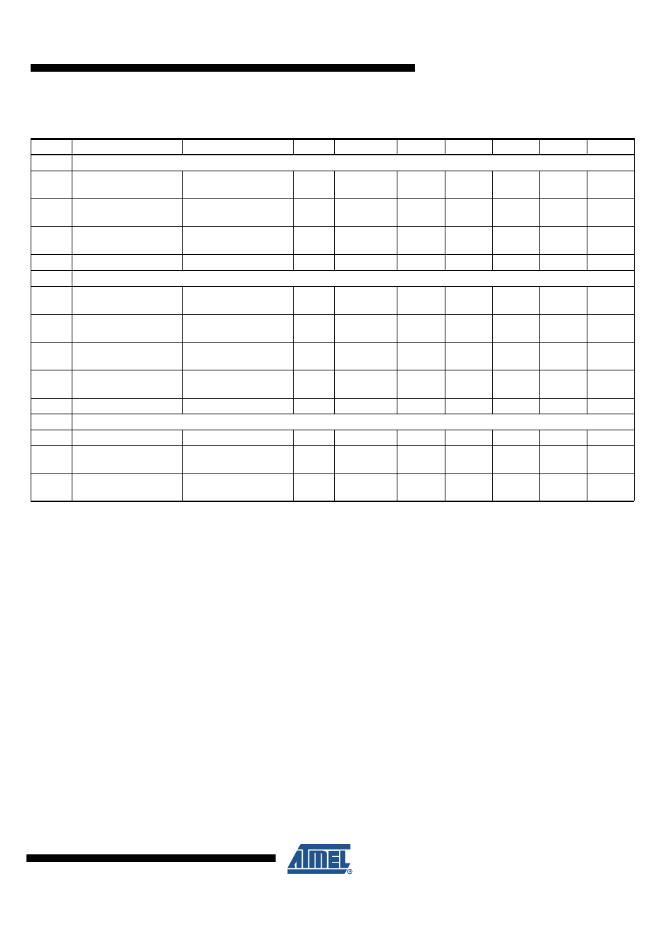
6
Inhibit Input
6.1
Input voltage low-level
threshold
V
IL
0.3
×
V
VCC
V
A
6.2
Input voltage high-level
threshold
V
IH
0.7
×
V
VCC
V
A
6.3
Hysteresis of input
voltage
∆
V
I
100
700
mV
A
6.4
Pull-down current
V
INH
= V
VCC
I
PD
10
80
µA
A
7
Serial Interface: Logic Inputs DI, CLK, CS
7.1
Input voltage low-level
threshold
V
IL
0.3
×
V
VCC
V
A
7.2
Input voltage high-level
threshold
V
IH
0.7
×
V
VCC
V
A
7.3
Hysteresis of input
voltage
∆
V
I
50
500
mV
A
7.4
Pull-down current pin
DI, CLK
V
DI
, V
CLK
= V
VCC
I
PDSI
2
50
µA
A
7.5
Pull-up current pin CS
V
CS
= 0V
I
PUSI
–50
–2
µA
A
8
Serial Interface: Logic Output DO
8.1
Output voltage low level I
OL
= 3 mA
V
DOL
0.5
V
A
8.2
Output voltage high
level
I
OL
= –1 mA
V
DOH
V
VCC
–
0.7V
V
A
8.3
Leakage current
(tri-state)
V
CS
= V
VCC,
0V < V
DO
< V
VCC
I
DO
–10
10
µA
A
7.
Electrical Characteristics (Continued)
7.5V < V
S
< 40V; 3V < V
CC
< 5.5V; INH = High; –40°C < T
j
< 200°C, T
a
≤
150°C; unless otherwise specified, all values refer to GND pins.
No.
Parameters
Test Conditions
Pin
Symbol
Min.
Typ.
Max.
Unit
Type*
*) Type means: A = 100% tested, B = 100% correlation tested, C = Characterized on samples, D = Design parameter
Notes:
1. Delay time between rising edge of input signal at pin CS after data transmission and switch on/off output stages to 90% of
final level. Device not in standby for t > 1 ms.