Ata6837 [preliminary, Pin configuration – Rainbow Electronics ATA6837 User Manual
Page 3
3
4953C–AUTO–09/07
ATA6837 [Preliminary]
2.
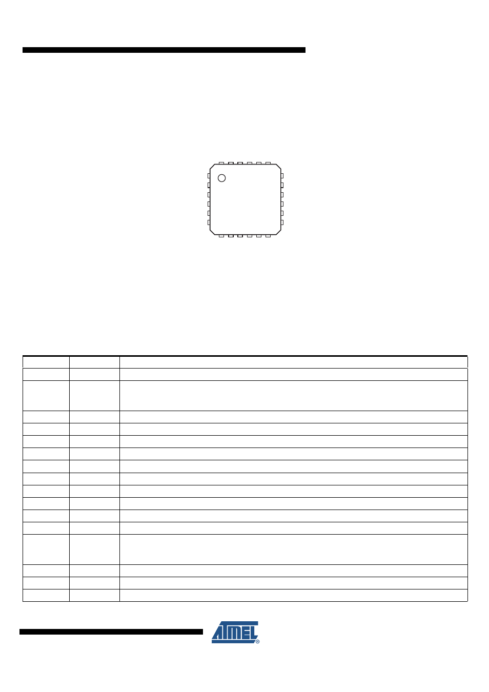
Pin Configuration
Figure 2-1.
Pinning QFN 24, 5
×
5, 0.65 mm pitch
Note:
YWW
Date code (Y = Year above 2000, WW = week number)
ATAxyz Product
name
ZZZZZ
Wafer lot number
AL
Assembly sub-lot number
OUT4 SENSE
OUT4
VS
VS
OUT3
OUT3 SENSE
CLK
CS
GND SENSE
NC
VCC
DO
NC
OUT5
OUT5 SENSE
OUT6 SENSE
OUT6
DI
NC
OUT2
OUT2 SENSE
OUT1 SENSE
OUT1
INH
1
2
3
4
5
6
18
17
16
15
14
13
7 8
9 10
12
11
24 23 22 21
19
20
Table 2-1.
Pin Description QFN24
Pin
Symbol
Function
1
OUT4 SENSE Only for testability in final test
2
OUT4
Half-bridge output 4; formed by internally connected power MOS high-side switch 4 and low-side switch 4
with internal reverse diodes; short circuit protection; overtemperature protection; diagnosis for short and
open load
3
VS
Power supply output stages HS4, HS5 and HS6
4
VS
Power supply output stages HS1, HS2 and HS3
5
OUT3
Output 3; see pin 1
6
OUT3 SENSE Only for testability in final test
7
NC
Internal bond to GND
8
OUT2
Output 2; see pin 1
9
OUT2 SENSE Only for testability in final test
10
OUT1 SENSE Only for testability in final test
11
OUT1
Output 1; see pin 1
12
INH
Inhibit input; 5V/3.3V logic input with internal pull down; low = standby, high = normal operation
13
DO
Serial data output; 5V/3.3V CMOS logic level tri-state output for output (status) register data; sends 16-bit
status information to the microcontroller (LSB is transferred first). Output will remain tri-stated unless
device is selected by CS = low, therefore, several ICs can operate on one data output line only
14
VCC
Logic supply voltage (5V/3.3V)
15
NC
Internal bond to GND
16
GND SENSE Ground; reference potential; internal connection to the lead frame; cooling tab