3 digital pins, Digital pins, Table 21: digital pins – Rainbow Electronics 78M6631 User Manual
Page 27
DS_6631_056
78M6631 Data Sheet
Rev 1
27
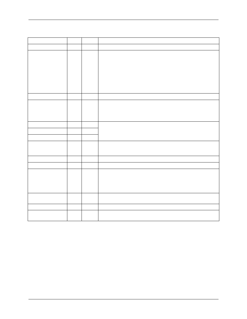
4.3 Digital Pins
Table 20: Digital Pins
Name
Type Circuit
Description
DIO3
I/O
3, 4 Dedicated DIO pin.
DIO4,DIO5,DIO6
DIO8, DIO9, DIO11
DIO17
DIO24, DIO25
DIO29, DIO30
DIO45, DIO47
DIO51, DIO53
DIO55
I/O
3, 4, 5 Multi-use pins, DIO.
(DIO4 = SCK, DIO5 = SDA when configured as EEPROM
interface;
If unused, these pins must be configured as DIOs
and set to outputs by the firmware.
D/Y
I
–
Selects either the Delta or the Wye configuration.
PCLK
PSDO
PCSZ
PSDI
I/O
3, 4, 5 SPI PORT.
E_RXTX
I/O
1, 4, 5 Port pins (when ICE_E pulled high).
E_RST
I/O
1, 4, 5
E_TCLK
O
4, 5
ICE_E
I
2
ICE enable. When zero, E_RST, E_TCLK and E_RXTX SEG32
For production units, this pin should be pulled to GND to disable
the emulator port.
CKTEST
I/O
3, 4 Test clock.
TMUXOUT
O
4
Digital test multiplexer output. Controlled by TMUX[3:0].
RESET
I
2
Chip reset: This input pin is used to reset the chip into a known
state. For normal operation, this pin is pulled low. To reset the
chip, this pin should be pulled high. This pin has an internal
30 µA (typ) current source pulldown. No external reset circuitry is
necessary.
RX
I
3
UART input.
If this pin is unused, it must be terminated to
V3P3D or GNDD.
TX
O
4
UART output.
GNDD (pin 55)
I
7
Enables Production Test.
This pin must be grounded in normal
operation.
Pin types: P = Power, O = Output, I = Input, I/O = Input/Output.
The circuit number denotes the equivalent circuit, as specified in Section 5, I/O Equivalent Circuits.