Ds1374, Table 3. square-wave output frequency – Rainbow Electronics DS1374 User Manual
Page 12
DS1374
Status Register (08h)
Bit 7/Oscillator Stop Flag (OSF). A logic 1 in this bit
indicates that the oscillator either is stopped or was
stopped for some period of time and can be used to
judge the validity of the timekeeping data. This bit is set
to logic 1 any time the oscillator stops. The following
are examples of conditions that can cause the OSF bit
to be set:
1) The first time power is applied.
2) The voltage present on V
CC
is insufficient to support
oscillation.
3) The
EOSC bit is turned off.
4) External influences on the crystal (i.e., noise, leak-
age, etc.).
This bit remains at logic 1 until written to logic 0.
Bit 0/Alarm Flag (AF). A logic 1 in the alarm flag bit
indicates that the WD/
ALM counter reached zero. If
WD/
ALM is set to zero and the AIE bit = 1, the INT pin
goes low and stays low until AF is cleared. AF is
cleared when written to logic 0. This bit can only be
written to logic 0. Attempting to write logic 1 leaves the
value unchanged. If WD/
ALM is set to 1 and the AIE
bit = 1, the
INT pin pulses low for 250ms when the
WD/
ALM counter reaches zero and sets AF = 1. At the
pulse completion, the DS1374 clears the AF bit to zero.
If the 250ms pulse is active, writing AF to zero does not
truncate the pulse.
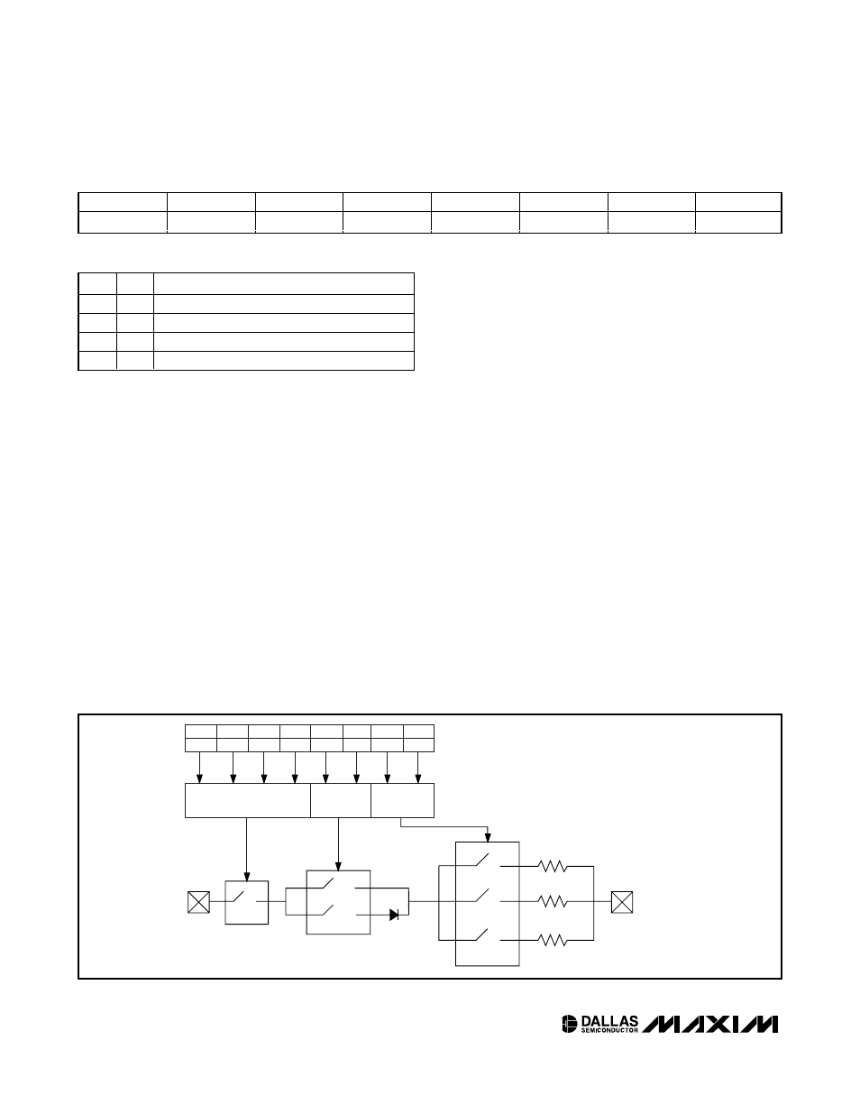
Trickle-Charge Register (10h)
The simplified schematic in Figure 7 shows the basic
components of the trickle charger. The trickle-charge
select (TCS) bits (bits 4–7) control the selection of the
trickle charger. To prevent accidental enabling, only a
pattern of 1010 enables the trickle charger. All other
patterns disable the trickle charger. The trickle charger
is disabled when power is first applied. The diode
select (DS) bits (bits 2, 3) select whether or not a diode
is connected between V
CC
and V
BACKUP
. If DS is 01,
no diode is selected; if DS is 10, a diode is selected.
The ROUT bits (bits 0, 1) select the value of the resistor
connected between V
CC
and V
BACKUP
. Table 4 shows
the resistor selected by the resistor select (ROUT) bits
and the diode selected by the diode select (DS) bits.
Warning: The ROUT value of 250
Ω must not be select-
ed whenever V
CC
is greater than 3.63V.
The user determines diode and resistor selection
according to the maximum current desired for battery or
super cap charging. The maximum charging current can
be calculated as illustrated in the following example.
I
2
C, 32-Bit Binary Counter Watchdog RTC with
Trickle Charger and Reset Input/Output
12
____________________________________________________________________
BIT 7
TCS3
1 OF 16 SELECT
NOTE: ONLY 1010b
ENABLES CHARGER
1 OF 2
SELECT
V
CC
V
BACKUP
R1
250
Ω
TCS
0-3
= TRICKLE CHARGER SELECT
DS
0-1
= DIODE SELECT
TOUT
0-1
= RESISTOR SELECT
R2
2k
Ω
R3
4k
Ω
1 OF 3
SELECT
BIT 6
TCS2
BIT 5
TCS1
BIT 4
TCS0
BIT 3
DS1
BIT 2
DS0
BIT 1
ROUT1
BIT 0
ROUT0
Figure 7. Programmable Trickle Charger
Bit 7
Bit 6
Bit 5
Bit 4
Bit 3
Bit 2
Bit 1
Bit 0
OSF
0
0
0
0
0
0
AF
RS2
RS1
SQUARE-WAVE OUTPUT FREQUENCY
0
0
1Hz
0
1
4.096kHz
1
0
8.192kHz
1
1
32.768kHz
Table 3. Square-Wave Output Frequency