Ds1374, Watchdog/alarm counter, Table 2. address map – Rainbow Electronics DS1374 User Manual
Page 10
DS1374
address range 00h–03h. When the counter is read, the
current time of day is latched into a register, which is
output on the serial data line while the counter contin-
ues to increment.
Watchdog/Alarm Counter
The contents of the watchdog/alarm counter, which is a
separate 24-bit down counter, are accessed in the
address range 04h–06h. When this counter is written, the
counter and a seed register are loaded with the desired
value. When the counter is to be reloaded, it uses the
value in the seed register. When the counter is read, the
current counter value is latched into a register, which is
output on the serial data line while the counter continues
to decrement.
If the counter is not needed, it can be disabled and used
as a 24-bit cache of NV RAM by setting the WACE bit in
the control register to logic 0. If all 24 bits of the watch-
dog/alarm counter are written to zero when
WACE = 1, the counter is disabled and the AF bit is
not set.
When the WD/
ALM bit in the control register is set to a
logic 0, the WD/
ALM counter decrements every second
until it reaches zero. At this point, the AF bit in the status
register is set and the counter is reloaded and restarted.
If AF is set when the watchdog function is enabled, the
output selected by WDSTR immediately becomes active.
When the WD/
ALM bit is set to logic 1, the WD/ALM
counter decrements every 1/4096 of a second (approxi-
mately every 244µs) until it reaches zero, sets the AF bit
in the status register, and stops. If WDSTR = 0, the
RST
pin pulses low for 250ms, and accesses to the DS1374
are inhibited. At the end of the 250ms pulse, the AF bit is
cleared to zero, the
RST pin becomes high impedance,
and read/write access to the DS1374 is enabled. If AIE =
1 and WDSTR = 1, the
INT pin pulses low for 250ms. The
pulse cannot be truncated by writing either AF or AIE to
zero during the low time of the
INT pin. If the WD/ALM
counter is written during the 250ms pulse, the counter
starts decrementing upon the pulse completion. At the
completion, the AF bit clears to zero and the
INT pin
becomes high impedance. The WD/
ALM counter can be
reloaded and restarted before the counter reaches zero
by reading or writing any of the WD/
ALM counter regis-
ters.
Power-Up/Power-Down Reset and
Pushbutton Reset Functions
A precision temperature-compensated reference and
comparator circuit monitors the status of V
CC
. When an
out-of-tolerance condition occurs, an internal power-fail
signal is generated that forces the
RST pin low and
blocks read/write access to the DS1374. When V
CC
returns to an in-tolerance condition, the
RST pin is held
low for 250ms to allow the power supply to stabilize. If
the
EOSC bit is set to a logic 1 (to disable the oscillator in
battery-backup mode), the reset signal is kept active for
250ms plus the startup time of the oscillator.
The DS1374 provides for a pushbutton switch to be con-
nected to the
RST output pin. When the DS1374 is not in
a reset cycle, it continuously monitors the
RST signal for
a low-going edge. If an edge is detected, the DS1374
debounces the switch by pulling the
RST pin low and
inhibits read/write access. After the internal 250ms timer
has expired, the device continues to monitor the
RST
line. If the line is still low, the DS1374 continues to moni-
tor the line, looking for a rising edge. Upon detecting
release, the DS1374 forces the
RST pin low and holds it
low for an additional 250ms.
I
2
C, 32-Bit Binary Counter Watchdog RTC with
Trickle Charger and Reset Input/Output
10
____________________________________________________________________
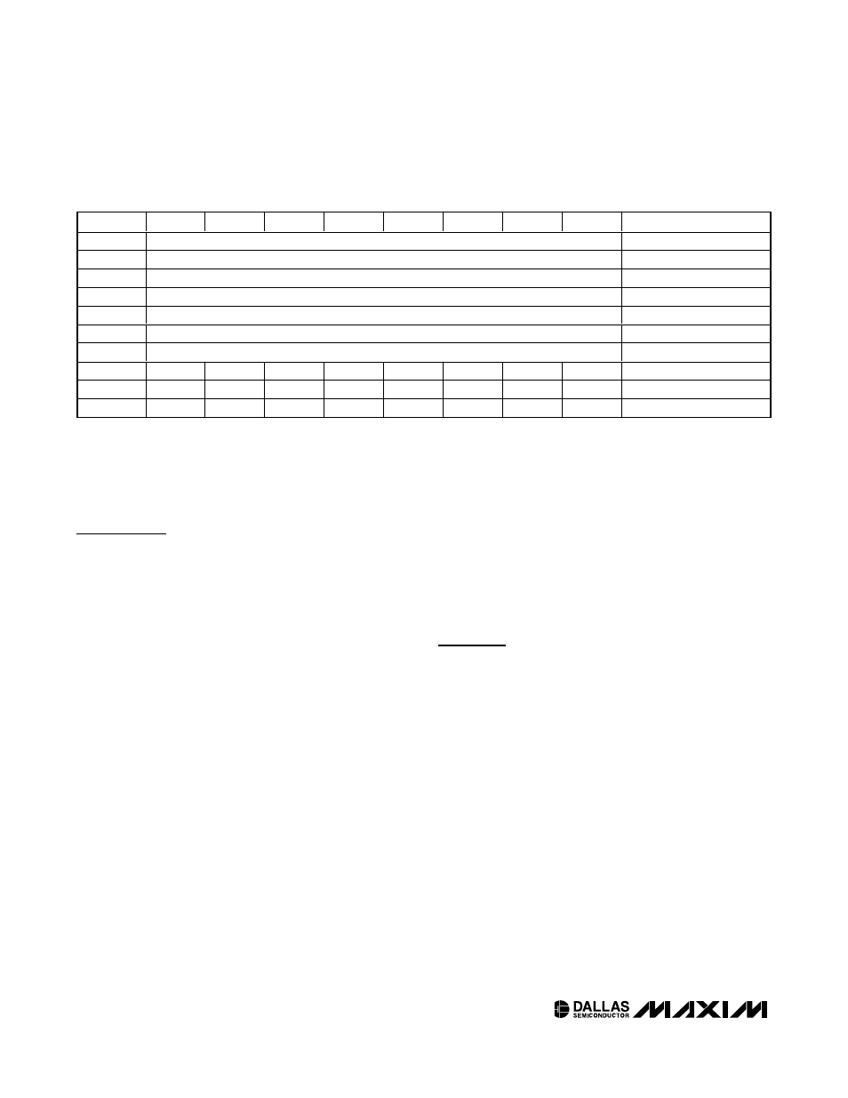
ADDRESS
BIT 7
BIT 6
BIT 5
BIT 4
BIT 3
BIT 2
BIT 1
BIT 0
FUNCTION
00H
TOD Counter Byte 0
Time-of-Day Counter
01H
TOD Counter Byte 1
Time-of-Day Counter
02H
TOD Counter Byte 2
Time-of-Day Counter
03H
TOD Counter Byte 3
Time-of-Day Counter
04H
WD/
ALM Counter Byte 0
Watchdog/Alarm Counter
05H
WD/
ALM Counter Byte 1
Watchdog/Alarm Counter
06H
WD/
ALM Counter Byte 2
Watchdog/Alarm Counter
07H
EOSC
WACE
WD/
ALM
BBSQW
WDSTR
RS2
RS1
AIE
Control
08H
OSF
0
0
0
0
0
0
AF
Status
09H
TCS3
TCS2
TCS1
TCS0
DS1
DS0
ROUT1
ROUT0
Trickle Charger
Table 2. Address Map
Note: Unless otherwise specified, the state of the registers is not defined when power is first applied.