Rainbow Electronics ATA6626 User Manual
Page 12
12
4970A–AUTO–01/07
ATA6621/22/24 Development Board
4.
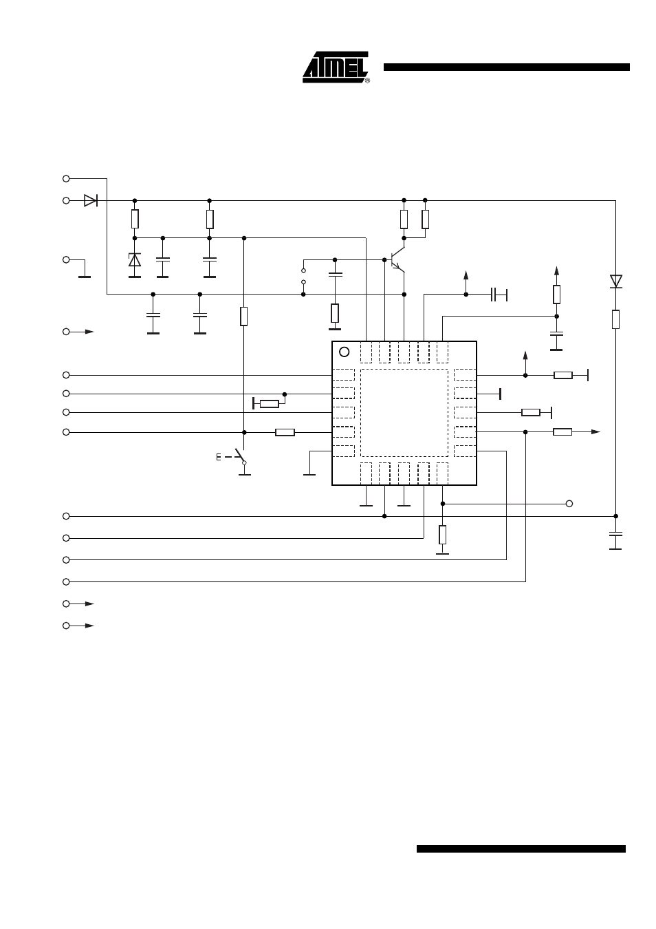
Schematic and Layout of the Development Board for the ATA6621/22/24
Figure 4-1.
Schematic of the Development Board for the ATA6621/22/24
Notes:
1. D3 and R4 are only necessary for a master node.
2. R9 and R13 are only needed for ATA6622 and ATA6624.
3. Pin KL_15 and the corresponding external circuitry are only available at the ATA6622/24.
4. Pin INH and the corresponding external circuitry are only available at the ATA6622/24.
5. Pin 17 has to be connected to GND by replacing C7 with a 0
Ω
resistor at ATA6622 or
ATA6624.
6. ATA6621: Pin 10 has to be connected to GND via R11 = 0. Pin 16 has to be connected to
GND by replacing C8 by a 0
Ω
resistor.
6
7
8
10
9
20
19
18
ATA6621/
ATA6622/
ATA6624
16
11
12
13
14
15
TXD
NRES
PVCC
LIN
WD_OSC
TM
MODE
GND
TEMP
PVCC
VCC
VS
NC
RXD
NC
LIN
NC
GND
WAKE
S1
Wake
R3
R5
R7
R8b
0
R8
100
Ω
/1W
R6
R13
0
51 k
Ω
3.3
Ω
33 k
Ω
10 k
Ω
NTRIG
PTRIG
EN
5
4
3
2
1
17
+
220 pF
C6
100 nF
1 nF
C8
C7
C4
C3
10 µF
22 µF/50V
C5
J1
VCC
V1
TEMP
VS
T1
MJD31C
2.2 µF
+
100 nF
C2
BZG04-33
LL4148
VBAT
GND
PVCC
D2
D1
C1
100 nF
+
0
R10b
R1
MODE
KL_15
(ATA6622/24)
INH
(ATA6622/24)
4.7 k
Ω
R9
10 k
Ω
R12
47 k
Ω
R10
10
Ω
/2W
R11
47 k
Ω
R4
D3
LL4148
1 k
Ω
TEMP
TEMP
EN
PTRIG
NTRIG
WAKE
MODE
KL_15
X1
LIN
RXD
TXD
NRES
MODE
KL_15
ATA6621-EK
Revision 2.0
ATA6622-EK
ATA6624-EK
GND
GND
GND
GND
KL15
INH