Input diagram, I/o diagram, Speed/power management – Rainbow Electronics ATF1502ASL User Manual
Page 6: Atf1502as(l)
6
ATF1502AS(L)
0995J–PLD–09/02
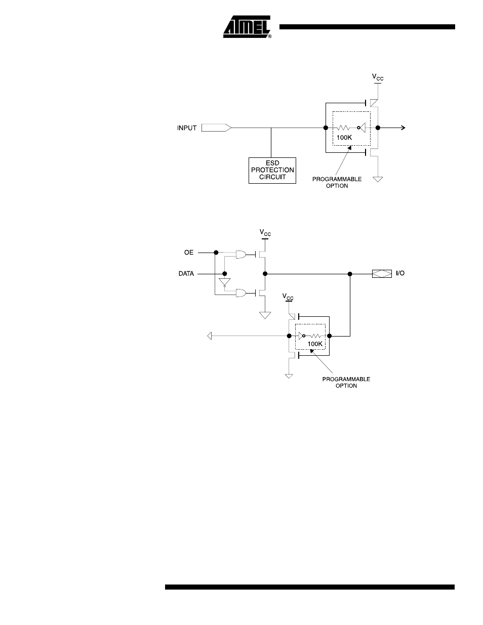
Input Diagram
I/O Diagram
Speed/Power
Management
The ATF1502AS has several built-in speed and power management features. The
ATF1502AS contains circuitry that automatically puts the device into a low-power standby
mode when no logic transitions are occurring. This not only reduces power consumption dur-
ing inactive periods, but also provides proportional power savings for most applications
running at system speeds below 50 MHz. This feature may be selected as a design option.
To further reduce power, each ATF1502AS macrocell has a reduced-power bit feature. This
feature allows individual macrocells to be configured for maximum power savings. This feature
may be selected as a design option.
The ATF1502AS also has an optional power-down mode. In this mode, current drops to below
10 mA. When the power-down option is selected, either PD1 or PD2 pins (or both) can be
used to power down the part. The power-down option is selected in the design source file.
When enabled, the device goes into power-down when either PD1 or PD2 is high. In the
power-down mode, all internal logic signals are latched and held, as are any enabled outputs.