Ac characteristics(1), Atf1502as(l), Ac characteristics – Rainbow Electronics ATF1502ASL User Manual
Page 15
15
ATF1502AS(L)
0995J–PLD–09/02
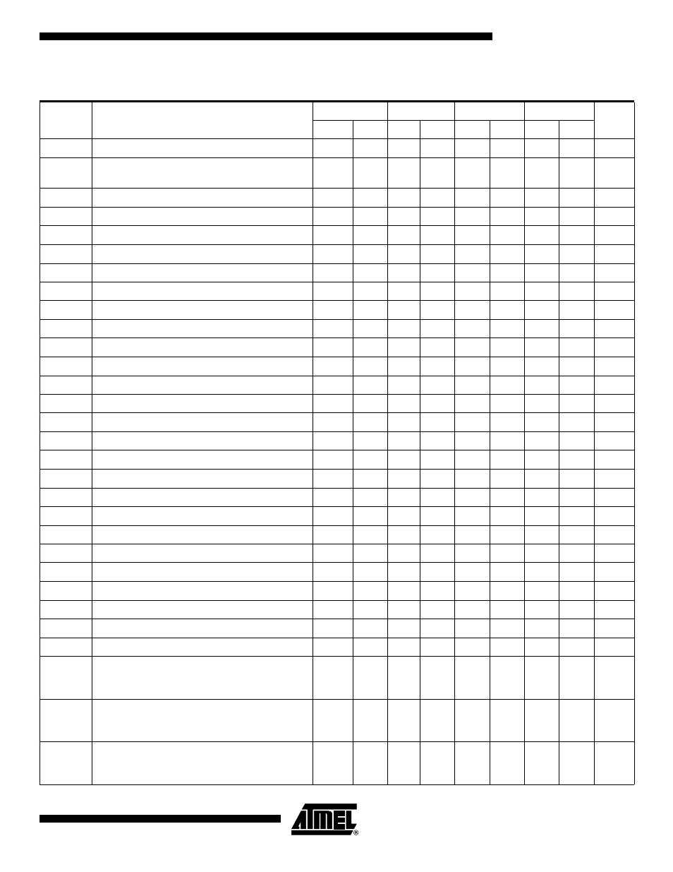
AC Characteristics
(1)
Symbol
Parameter
-7
-10
-15
-25
Units
Min
Max
Min
Max
Min
Max
Min
Max
t
PD1
Input or Feedback to Non-registered Output
7.5
10
3
15
25
ns
t
PD2
I/O Input or Feedback to Non-registered
Feedback
7
9
3
12
25
ns
t
SU
Global Clock Setup Time
6
7
11
20
ns
t
H
Global Clock Hold Time
0
0
0
0
ns
t
FSU
Global Clock Setup Time of Fast Input
3
3
3
5
ns
t
FH
Global Clock Hold Time of Fast Input
0.5
0.5
1
2
MHz
t
COP
Global Clock to Output Delay
4.5
5
8
13
ns
t
CH
Global Clock High Time
3
4
5
7
ns
t
CL
Global Clock Low Time
3
4
5
7
ns
t
ASU
Array Clock Setup Time
3
3
4
5
ns
t
AH
Array Clock Hold Time
2
3
4
6
ns
t
ACOP
Array Clock Output Delay
7.5
10
15
25
ns
t
ACH
Array Clock High Time
3
4
6
10
ns
t
ACL
Array Clock Low Time
3
4
6
10
ns
t
CNT
Minimum Clock Global Period
8
10
13
22
ns
f
CNT
Maximum Internal Global Clock Frequency
125
100
76.9
50
MHz
t
ACNT
Minimum Array Clock Period
8
10
13
22
ns
f
ACNT
Maximum Internal Array Clock Frequency
125
100
76.9
50
MHz
f
MAX
Maximum Clock Frequency
166.7
125
100
60
MHz
t
IN
Input Pad and Buffer Delay
0.5
0.5
2
2
ns
t
IO
I/O Input Pad and Buffer Delay
0.5
0.5
2
2
ns
t
FIN
Fast Input Delay
1
1
2
2
ns
t
SEXP
Foldback Term Delay
4
5
8
12
ns
t
PEXP
Cascade Logic Delay
0.8
0.8
1
2
ns
t
LAD
Logic Array Delay
3
5
6
8
ns
t
LAC
Logic Control Delay
3
5
6
8
ns
t
IOE
Internal Output Enable Delay
2
2
3
4
ns
t
OD1
Output Buffer and Pad Delay
(Slow slew rate = OFF;
V
CC
= 5V; C
L
= 35 pF)
2
1.5
4
6
ns
t
ZX1
Output Buffer Enable Delay
(Slow slew rate = OFF;
V
CCIO
= 5.0V; C
L
= 35 pF)
4.0
5.0
7
10
ns
t
ZX2
Output Buffer Enable Delay
(Slow slew rate = OFF;
V
CCIO
= 3.3V; C
L
= 35 pF)
4.5
5.5
7
10
ns