Note 3), Note 4), Note 5) – Rainbow Electronics ADC081000 User Manual
Page 9: Note 8), Note 9), Note 10), Note 12), Note 13), Note 11), Converter electrical characteristics
Converter Electrical Characteristics
(Continued)
The following specifications apply after calibration for V
A
= V
DR
= +1.9V
DC
, OutV = 1.9V, V
IN
FSR (a.c. coupled) = differential
800mV
P-P
, C
L
= 10 pF, Differential, a.c. coupled Sinewave Clock, f
CLK
= 1 GHz at 0.5V
P-P
with 50% duty cycle, R
EXT
= 3300
Ω
±
0.1%, Analog Signal Source Impedance = 100
Ω. Boldface limits apply for T
A
= T
MIN
to T
MAX
. All other limits T
A
= 25˚C,
unless otherwise stated. (Notes 6, 7)
Symbol
Parameter
Conditions
Typical
Limits
Units
(Limits)
AC ELECTRICAL CHARACTERISTICS
t
AJ
Aperture Jitter
0.4
ps rms
t
OD
Input Clock to Data Output Delay
50% of Input Clock transition to
50% of Data transition
2.7
ns
Pipeline Delay (Latency) (Note 11)
"D" Outputs
7
Clock Cycles
"Dd" Outputs
8
t
WU
PD low to Rated Accuracy
Conversion (Wake-Up Time)
500
ns
t
CAL
Calibration Cycle Time
46,000
Clock Cycles
Note 1: Absolute Maximum Ratings indicate limits beyond which damage to the device may occur. There is no guarantee of operation at the Absolute Maximum
Ratings. Operating Ratings indicate conditions for which the device is functional, but do not guarantee specific performance limits. For guaranteed specifications and
test conditions, see the Electrical Characteristics. The guaranteed specifications apply only for the test conditions listed. Some performance characteristics may
degrade when the device is not operated under the listed test conditions.
Note 2: All voltages are measured with respect to GND = DR GND = 0V, unless otherwise specified.
Note 3: When the input voltage at any pin exceeds the power supply limits (that is, less than GND or greater than V
A
), the current at that pin should be limited to
25 mA. The 50 mA maximum package input current rating limits the number of pins that can safely exceed the power supplies with an input current of 25 mA to two.
This limit is not placed upon the power, ground and digital output pins.
Note 4: Human body model is 100 pF capacitor discharged through a 1.5 k
Ω resistor. Machine model is 220 pF discharged through ZERO Ohms.
Note 5: See AN-450, “Surface Mounting Methods and Their Effect on Product Reliability”.
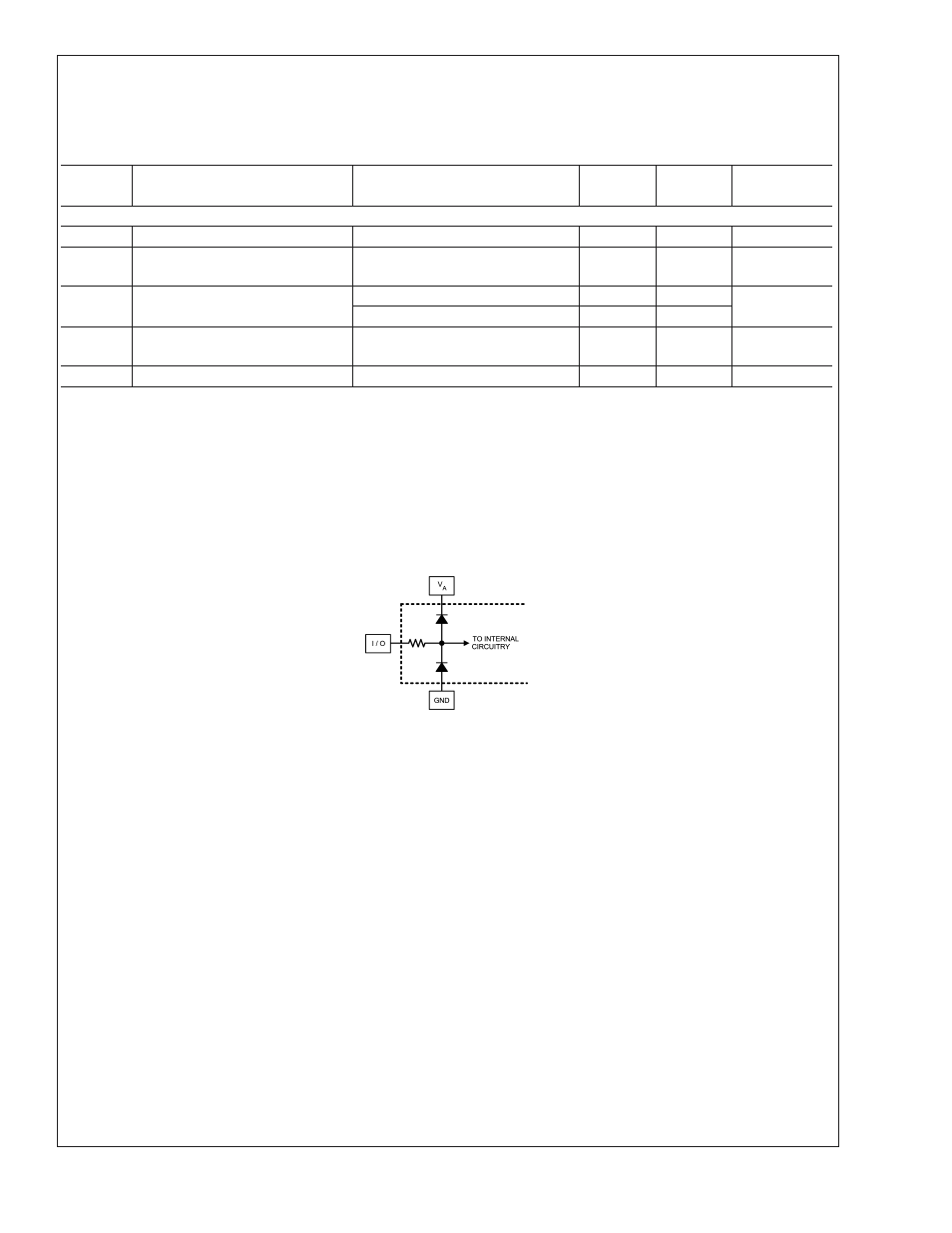
Note 6: The analog inputs are protected as shown below. Input voltage magnitudes beyond the Absolute Maximum Ratings may damage this device.
20068104
Note 7: To guarantee accuracy, it is required that V
A
and V
DR
be well bypassed. Each supply pin must be decoupled with separate bypass capacitors. Additionally,
achieving rated performance requires that the backside exposed pad be well grounded.
Note 8: Typical figures are at T
J
= 25˚C, and represent most likely parametric norms. Test limits are guaranteed to National’s AOQL (Average Outgoing Quality
Level).
Note 9: Calculation of Full-Scale Error for this device assumes that the actual reference voltage is exactly its nominal value. Full-Scale Error for this device,
therefore, is a combination of Full-Scale Error and Reference Voltage Error. See Transfer Characteristic Figure 2. For relationship between Gain Error and Full-Scale
Error, see Specification Definitions for Gain Error.
Note 10: The analog and clock input capacitances are die capacitances only. Additional package capacitances of 0.65 pF differential and 0.95 pF each pin to ground
are isolated from the die capacitances by lead and bond wire inductances.
Note 11: This parameter is guaranteed by design and is not tested in production.
Note 12: This parameter is guaranteed by design and characterization and is not tested in production.
Note 13: The digital control pin capacitances are die capacitances only. Additional package capacitance of 1.6 pF each pin to ground are isolated from the die
capacitances by lead and bond wire inductances.
Note 14: The ADC081000 has two interleaved LVDS output buses, which each clock data out at one half the sample rate. The data at each bus is clocked out at
one half the sample rate. The second bus (D0 through D7) has a pipeline latency that is one clock cycle less than the latency of the first bus (Dd0 through Dd7).
ADC081000
www.national.com
9