Converter electrical characteristics – Rainbow Electronics ADC081000 User Manual
Page 8
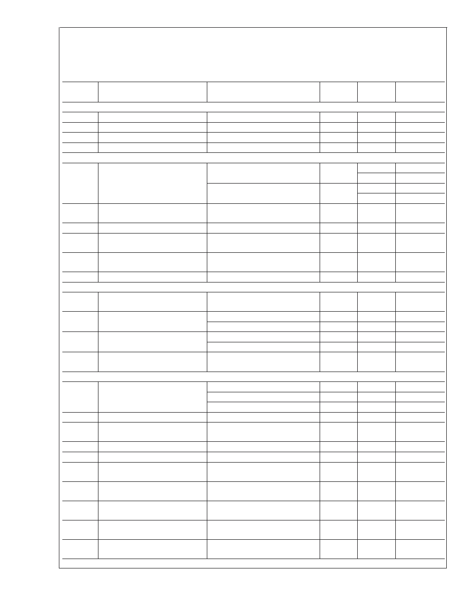
Converter Electrical Characteristics
(Continued)
The following specifications apply after calibration for V
A
= V
DR
= +1.9V
DC
, OutV = 1.9V, V
IN
FSR (a.c. coupled) = differential
800mV
P-P
, C
L
= 10 pF, Differential, a.c. coupled Sinewave Clock, f
CLK
= 1 GHz at 0.5V
P-P
with 50% duty cycle, R
EXT
= 3300
Ω
±
0.1%, Analog Signal Source Impedance = 100
Ω. Boldface limits apply for T
A
= T
MIN
to T
MAX
. All other limits T
A
= 25˚C,
unless otherwise stated. (Notes 6, 7)
Symbol
Parameter
Conditions
Typical
Limits
Units
(Limits)
DIGITAL CONTROL PIN CHARACTERISTICS
V
IH
Logic High Input Voltage
1.4
V (min)
V
IL
Logic Low Input Voltage
0.5
V (max)
I
I
Input Current
V
IN
= 0 or V
IN
= V
A
±
1
µA
C
IN
Logic Input Capacitance (Note 13)
Each input to ground
1.2
pF
DIGITAL OUTPUT CHARACTERISTICS
V
OD
LVDS Differential Output Voltage
OutV = V
A
, measured single-ended
300
200
mV
P-P
(min)
450
mV
P-P
(max)
OutV = GND, measured
single-ended
225
140
mV
P-P
(min)
340
mV
P-P
(max)
∆ V
OD
DIFF
Change in LVDS Output Swing
Between Logic Levels
±
1
mV
V
OS
Output Offset Voltage
800
mV
∆ V
OS
Output Offset Voltage Change
Between Logic Levels
±
1
mV
I
OS
Output Short Circuit Current
Output+ & Output- connected to
0.8V
−4
mA
Z
O
Differential Output Impedance
100
Ohms
POWER SUPPLY CHARACTERISTICS
I
A
Analog Supply Current
PD = Low
PD = High
646
4.5
792
mA (max)
mA
I
DR
Output Driver Supply Current
PD = Low
108
160
mA (max)
PD = High
0.1
mA
P
D
Power Consumption
PD = Low
1.43
1.8
W (max)
PD = High
8.7
mW
PSRR1
D.C. Power Supply Rejection Ratio
Change in Offset Error with change
in V
A
from 1.8V to 2.0V
73
dB
AC ELECTRICAL CHARACTERISTICS
f
CLK1
Maximum Conversion Rate
T
A
= 85˚C
1.1
1.0
GHz (min)
T
A
≤ 75˚C
1.3
GHz
T
A
≤ 70˚C
1.6
GHz
f
CLK2
Minimum Conversion Rate
200
MHz
Input Clock Duty Cycle
200 MHz
≤ Input clock frequency
<
1 GHz
50
20
80
% (min)
% (max)
t
CL
Input Clock Low Time (Note 12)
500
200
ps (min)
t
CH
Input Clock High Time (Note 12)
500
200
ps (min)
DCLK Duty Cycle (Note 12)
50
45
55
% (min)
% (max)
t
LHT
Differential Low to High Transition
Time
10% to 90%, C
L
= 2.5 pF
250
ps
t
HLT
Differential High to Low Transition
Time
10% to 90%, C
L
= 2.5 pF
250
ps
t
OSK
DCLK to Data Output Skew
50% of DCLK transition to 50% of
Data transition
0
±
200
ps (max)
t
AD
Sampling (Aperture) Delay
Input CLK+ Fall to Acquisition of
Data
930
ps
ADC081000
www.national.com
8