4 clocking, 5 the lvds outputs, 6 out of range (or) indication – Rainbow Electronics ADC081000 User Manual
Page 23: 7 power down, 8 summary of control pins and convenience outputs, Table 1. digital control pins, Table 2. convenience output pins, Applications information, 0 the reference voltage, 0 the analog input
Functional Description
(Continued)
1.4 Clocking
The ADC081000 must be driven with an a.c. coupled, differ-
ential clock signal. Section 4 describes the use of the clock
input pins. A differential LVDS output clock is available for
use in latching the ADC output data into whatever receives
that data.
To help ease data capture, the output data may be caused to
transition on either the positive or the negative edge of the
output data clock (DCLK). This is chosen with the OutEdge
input. A high on the OutEdge input causes the output data to
transition on the rising edge of DCLK, while grounding this
input causes the output to transition on the falling edge of
DCLK.
1.5 The LVDS Outputs
The data outputs, the Out Of Range (OR) and DCLK are
LVDS compliant outputs. Output current sources provide 3
mA of output current to a differential 100 Ohm load when the
OutV input is high or 2.2 mA when the OutV input is low. For
short LVDS lines and low noise systems, satisfactory perfor-
mance may be realized with the OutV input low, which
results in lower power consumption. If the LVDS lines are
long and/or the system in which the ADC081000 is used is
noisy, it may be necessary to tie the OutV pin high.
1.6 Out Of Range (OR) Indication
The input signal is out of range whenever the correct code
would be above positive full-scale or below negative full
scale. When the input signal for any given sample is thus out
of range, the OR output is high for that word time.
1.7 Power Down
The ADC081000 is in the active state when the Power Down
pin (PD) is low. When the PD pin is high, the device is in the
power down mode, where the device power consumption is
reduced to a minimal level and the outputs are in a high
impedance state. Upon return to normal operation, the pipe-
line will contain meaningless information and must be
flushed.
If the PD input is brought high while a calibration is running,
the device will not go into power down until the calibration
sequence is complete. However, if power is applied and PD
is already high, the device will not begin the calibration
sequence until the PD input goes low. If a manual calibration
is requested while the device is powered down, the calibra-
tion will not begin at all. That is, the manual calibration input
is completely ignored in the power down state.
1.8 Summary of Control Pins and Convenience
Outputs
Table 1 and Table 2 are provided as a guide to the use of the
various control and convenience pins of the ADC081000.
Note that this table is only a guide and that the rest of this
data sheet should be consulted for the full meaning and use
of these pins.
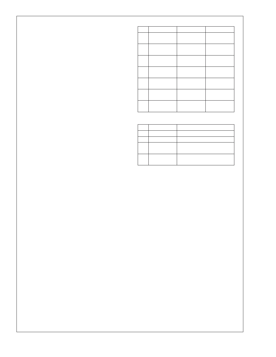
TABLE 1. Digital Control Pins
PIN
DESCRIPTION
LOW
HIGH
3
OutV
440mV Outputs
600mV
Outputs
4
OutEdge
Data Transition
at DCLK Fall
Data Transition
at DCLK Rise
14
DC_Coup
A.C. Coupled
Inputs
D.C. Coupled
Inputs
26
PD
Normal
Operation
Power Down
30
CAL
Normal
Operation
Run
Calibration
35
FSR
600 mV
P-P
Full-Scale In
800 mV
P-P
Full-Scale In
127
CalDly
2
24
Clock
Cycles
2
30
Clock
Cycles
TABLE 2. Convenience Output Pins
PIN
DESCRIPTION
USE / INDICATION
7
V
CMO
Common Mode Output Voltage.
31
V
BG
1.25V Convenience Output.
79
80
OR+
OR−
Differential Out-Of-Range
Indication; active high.
126
CalRun
Low is normal operation. High
indicates Calibration is running.
Applications Information
2.0 THE REFERENCE VOLTAGE
The voltage reference for the ADC081000 is derived from a
1.254V bandgap reference which is made available at the
V
BG
output for user convenience and has an output current
capability of
±
100 µA. The V
BG
output should be buffered if
more current than this is required of it.
The internal bandgap-derived reference voltage causes the
full-scale peak-to-peak input swing to be either 600 mV or
800 mV, as determined by the FSR pin and described in
Section 1.3. There is no provision for the use of an external
reference voltage.
3.0 THE ANALOG INPUT
The analog input is a differential one to which the signal
source may be a.c. coupled or d.c. coupled. Table 3 gives
the input to output relationship with the FSR pin high. With
the FSR pin grounded, the millivolt values in Table 3 are
reduced to 75% of the values indicated.
The buffered analog inputs simplify the task of driving these
inputs and the RC pole that is generally used at sampling
ADC inputs is not required. If it is desired to use an amplifier
circuit before the ADC, use care in choosing an amplifier with
adequate noise and distortion performance and adequate
gain at the frequencies used for the application.
ADC081000
www.national.com
23