2 calibration delay, 3 output edge synchronization, 4 power down feature – Rainbow Electronics ADC081000 User Manual
Page 26: 0 the digital outputs, 0 power considerations, 1 supply voltage, Figure 8. non-spiking power supply, Applications information
Applications Information
(Continued)
5.2 Calibration Delay
The CalDly input (pin 127) is used to select one of two delay
times after the application of power to the start of calibration,
as described in Section 1.1. The calibration delay values
allow the power supply to come up and stabilize before
calibration takes place. With no delay or insufficient delay,
calibration would begin before the power supply is stabilized
at its operating value and result in non-optimal calibration
coefficients. If the PD pin is high upon power-up, the calibra-
tion delay counter will be disabled until the PD pin is brought
low. Therefore, holding the PD pin high during power up will
further delay the start of the power-up calibration cycle. The
best setting of the CalDly pin depends upon the power-on
settling time of the power supply.
5.3 Output Edge Synchronization
DCLK signals are available to help latch the converter output
data into external circuitry. The output data can be synchro-
nized with either edge of these clock signals. That is, the
output data transition can be set to occur with either the
rising edge or the falling edge of the DCLK signal, so that
either edge of that clock signal can be used to latch the
output data into the receiving circuit.
When the OutEdge pin is high, the output data is synchro-
nized with (changes with) the rising edge of DCLK+. When
OutEdge is low, the output data is synchronized with the
falling edge of DCLK+.
At the very high speeds of which the ADC081000 is capable,
slight differences in the lengths of the clock and data lines
can mean the difference between successful and erroneous
data capture. The OutEdge pin is used to capture data on
the DCLK edge that best suits the application circuit and
layout.
5.4 Power Down Feature
The Power Down (PD) pin, when high, puts the ADC081000
into a low power mode where power consumption is greatly
reduced.
The digital output pins retain the last conversion output code
when the clock is stopped, but are in a high impedance state
when the PD pin is high. However, upon return to normal
operation (re-establishment of the clock and/or lowering of
the PD pin), the pipeline will contain meaningless informa-
tion and must be flushed.
If the PD input is brought high while a calibration is running,
the device will not go into power down until the calibration
sequence is complete. However, if power is applied and PD
is already high, the device will not begin the calibration
sequence until the PD input goes low. If a manual calibration
is requested while the device is powered down, the calibra-
tion will not begin at all. That is, the manual calibration input
is completely ignored in the power down state.
6.0 THE DIGITAL OUTPUTS
The ADC081000 demultiplexes its output data onto two
LVDS output buses.
The results of successive conversions started on the odd
falling edges of the CLK+ pin are available on one of the two
LVDS buses, while the results of conversions started on the
even falling edges of the CLK+ pin are available on the other
LVDS bus. This means that the word rate at each LVDS bus
is 1/2 the ADC081000 clock rate and the two buses must be
interleaved to obtain the entire 1 GSPS conversion result.
Since the minimum recommended clock rate for this device
is 200 MSPS, the effective sample rate can be reduced to as
low as 100 MSPS by using the results available on just one
of the the two LVDS buses and a 200 MHz input clock,
decimating the 200 MSPS data by two.
There is one LVDS clock pair available for use to latch the
LVDS outputs on both buses. Whether the data is sent at the
rising or falling edge of DCLK+ is determined by the sense of
the OutEdge pin, as described in Section 5.3.
The OutV pin is used to set the LVDS differential output
levels. See Section 1.5.
The output format is Offset Binary. Accordingly, a full-scale
input level with V
IN
+ positive with respect to V
IN
− will pro-
duce an output code of all ones, a full-scale input level with
V
IN
− positive with respect to V
IN
+ will produce an output
code of all zeros and when V
IN
+ and V
IN
− are equal, the
output code will vary between 127 and 128.
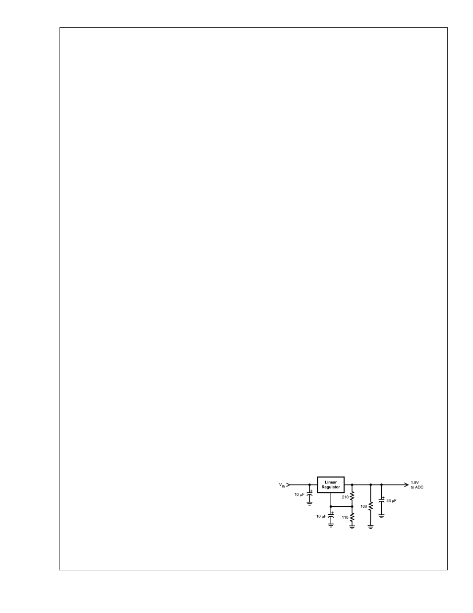
7.0 POWER CONSIDERATIONS
A/D converters draw sufficient transient current to corrupt
their own power supplies if not adequately bypassed. A 33
µF capacitor should be placed within an inch (2.5 cm) of the
A/D converter power pins. A 0.1 µF capacitor should be
placed as close as possible to each V
A
pin, preferably within
one-half centimeter. Leadless chip capacitors are preferred
because they have low lead inductance. Having power and
ground planes in adjacent layers of the PC Board will provide
the best supply bypass capacitance in terms of low ESL.
The V
A
and V
DR
supply pins should be isolated from each
other to prevent any digital noise from being coupled into the
analog portions of the ADC. A ferrite choke, such as the JW
Miller FB20009-3B, is recommended between these supply
lines when a common source is used for them.
As is the case with all high speed converters, the
ADC081000 should be assumed to have little power supply
noise rejection. Any power supply used for digital circuity in a
system where a lot of digital power is being consumed
should not be used to supply power to the ADC081000. The
ADC supplies should be the same supply used for other
analog circuitry, if not a dedicated supply.
7.1 Supply Voltage
The ADC081000 is specified to operate with a supply voltage
of 1.9V
±
0.1V. It is very important to note that, while this
device will function with slightly higher supply voltages,
these higher supply voltages may reduce product lifetime.
No pin should ever have a voltage on it that is in excess of
the supply voltage or below ground by more than 150 mV,
not even on a transient basis. This can be a problem upon
application of power and power shut-down. Be sure that the
supplies to circuits driving any of the input pins, analog or
digital, do not come up any faster than does the voltage at
the ADC081000 power pins.
20068154
FIGURE 8. Non-Spiking Power Supply
ADC081000
www.national.com
26