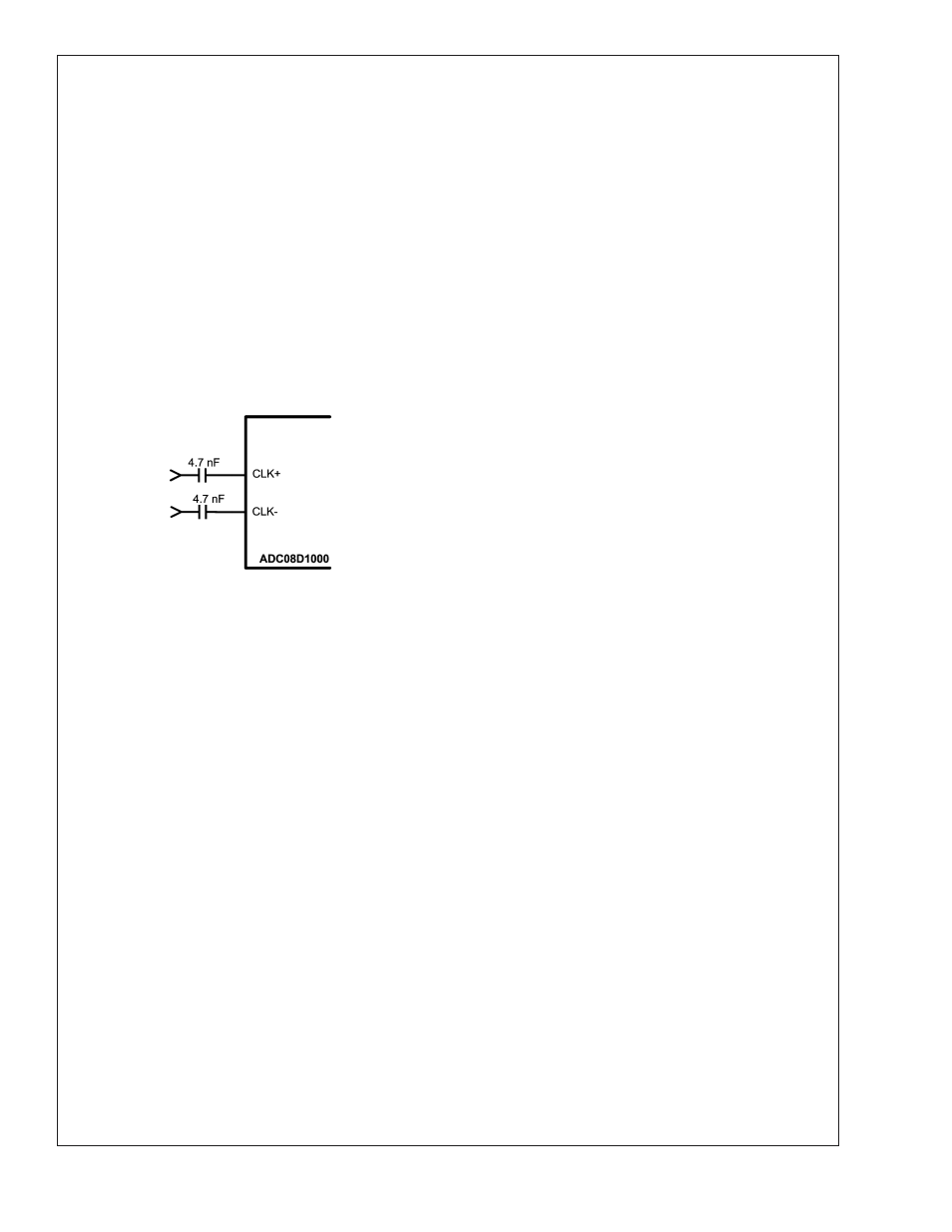
0 the clock inputs, Figure 7. differential (lvds) clock connection, 0 control pins – Rainbow Electronics ADC081000 User Manual
Page 25: 1 self calibration, 1 power-on calibration, 2 on-command calibration, Applications information
Applications Information
(Continued)
4.0 THE CLOCK INPUTS
The ADC081000 has differential LVDS clock inputs, CLK+
and CLK-, which must be driven with an a.c. coupled, differ-
ential clock signal. Although the ADC081000 is tested and its
performance is guaranteed with a differential 1.0 GHz clock,
it typically will function well with clock frequencies indicated
in the Electrical Characteristics Table. The clock inputs are
internally terminated and biased. The clock signal must be
capacitive coupled to the clock pins as indicated in Figure 7.
Operation up to the sample rates indicated in the Electrical
Characteristics Table is typically possible if the conditions of
the Operating Ratings are not exceeded. Operating at higher
sample rates than indicated for the given ambient tempera-
ture may result in reduced device reliability and product
lifetime. This is because of the higher power consumption
and die temperatures at high sample rates. Important also
for reliability is proper thermal management . See Section
7.2.
The differential Clock line pair should have a characteristic
impedance of 100
Ω and be terminated at the clock source in
that (100
Ω) characteristic impedance. The clock line should
be as short and as direct as possible. The ADC081000 clock
input is internally terminated with an untrimmed 100
Ω resis-
tor.
Insufficient clock levels will result in poor dynamic perfor-
mance. Excessively high clock levels could cause a change
in the analog input offset voltage. To avoid these problems,
keep the clock level within the range specified in the Oper-
ating Ratings.
While it is specified and performance is guaranteed at 1.0
GSPS with a 50% clock duty cycle, ADC081000 perfor-
mance is essentially independent of clock duty cycle. How-
ever, to ensure performance over temperature, it is recom-
mended that the input clock duty cycle be such that the
minimum clock high and low times are maintained within the
range specified in the Electrical Characteristics Table.
High
speed,
high
performance
ADCs
such
as
the
ADC081000 require very stable clock signals with minimum
phase noise or jitter. ADC jitter requirements are defined by
the ADC resolution (number of bits), maximum ADC input
frequency and the input signal amplitude relative to the ADC
input full scale range. The maximum jitter (the total of the
jitter from all sources) allowed to prevent a jitter-induced
reduction in SNR is found to be
t
J(MAX)
= (V
IN(P-P)
/V
INFSR
) x (1/(2
(N+1)
x
π x f
IN
))
where t
J(MAX)
is the rms total of all jitter sources in seconds,
V
IN(P-P)
is the peak-to-peak analog input signal, V
INFSR
is the
full-scale range of the ADC, "N" is the ADC resolution in bits
and f
IN
is the maximum input frequency, in Hertz, to the ADC
analog input.
Note that the maximum jitter described above is the rms total
of the jitter from all sources, including that in the ADC clock,
that added by the system to the ADC clock and input signals
and that added by the ADC itself. Since the effective jitter
added by the ADC is beyond user control, the best the user
can do is to keep the sum of the externally added clock jitter
and the jitter added by the analog circuitry to the analog
signal to a minimum.
5.0 CONTROL PINS
Seven control pins provide a wide range of possibilities in the
operation of the ADC081000 and facilitate its use. These
control pins provide Full-Scale Input Range setting, Self
Calibration, Calibration Delay, Output Edge Synchronization
choice, LVDS Output Level choice and a Power Down fea-
ture.
5.1 Self Calibration
The ADC081000 self-calibration must be run to achieve
rated performance. This procedure is performed upon
power-up and can be run any time on command. The cali-
bration procedure is exactly the same whether there is a
clock present upon power up or if the clock begins some time
after application of power. The CalRun output indicator is
high while a calibration is in progress.
5.1.1 Power-on Calibration
Power-on calibration begins after a time delay following the
application of power. This time delay is determined by the
setting of CalDly, as described in Section 1.1.
The calibration process will be not be performed if the CAL
pin is high at power up. In this case, the calibration cycle will
not begin until on-command calibration conditions are met.
The ADC081000 will function with the CAL pin held high at
power up, but no calibration will be done and performance
will be impaired. A manual calibration, however, may be
performed after powering up with the CAL pin high. See
On-Command Calibration Section 5.1.2.
The internal power-on calibration circuitry comes up in a
random state. If the clock is not running at power up and the
power on calibration circuitry is active, it will hold the analog
circuitry in power down and the power consumption will
typically be less than 200 mW. The power consumption will
be normal after the clock starts.
5.1.2 On-Command Calibration
Calibration may be run at any time by bringing the CAL pin
high for a minimum of 10 clock cycles after it has been low
for a minimum of 10 clock cycles. Holding the CAL pin high
upon power up will prevent execution of power-on calibration
until the CAL pin is low for a minimum of 10 clock clock
cycles, then brought high for a minimum of another 10 clock
cycles. The calibration cycle will begin 10 clock cycles after
the CAL pin is thus brought high.
The minimum 10 clock cycle sequences are required to
ensure that random noise does not cause a calibration to
begin when it is not desired. As mentioned in section 1.1, for
best performance, a self calibration should be performed 20
seconds or more after power up and repeated when the
ambient temperature changes more than 30˚C since the last
self calibration was run. SINAD drops about 1.5 dB for every
30˚C change in die temperature and ENOB drops about 0.25
bit for every 30˚C change in die temperature.
20068147
FIGURE 7. Differential (LVDS) Clock Connection
ADC081000
www.national.com
25