2 thermal management, Figure 9. recommended package land pattern, Applications information – Rainbow Electronics ADC081000 User Manual
Page 27
Applications Information
(Continued)
The Absolute Maximum Ratings should be strictly observed,
even during power up and power down. A power supply that
produces a voltage spike at turn-on and/or turn-off of power
can destroy the ADC081000. The circuit of Figure 8 will
provide supply overshoot protection.
Many linear regulators will produce output spiking at
power-on unless there is a minimum load provided. Active
devices draw very little current until their supply voltages
reach a few hundred millivolts. The result can be a turn-on
spike that can destroy the ADC081000, unless a minimum
load is provided for the supply. The 100
Ω resistor at the
regulator output in Figure 8 provides a minimum output
current during power-up to ensure there is no turn-on spik-
ing.
In this circuit, an LM317 linear regulator is satisfactory if its
input supply voltage is 4V to 5V . If a 3.3V supply is used, an
LM1086 linear regulator is recommended. Also, be sure that
the impedance of the power distribution system is low to
minimize resistive losses and minimize noise on the power
supply.
The output drivers should have a supply voltage, V
DR
, that is
within the range specified in the Operating Ratings table.
This voltage should not exceed the V
A
supply voltage.
If the power is applied to the device without a clock signal
present, the current drawn by the device might be below 100
mA. This is because the ADC081000 gets reset through
clocked logic and its initial state is random. If the reset logic
comes up in the "on" state, it will cause most of the analog
circuitry to be powered down, resulting in less than 100 mA
of current draw. This current is greater than the power down
current because not all of the ADC is powered down. The
device current will be normal after the clock is established.
7.2 Thermal Management
The ADC081000 is capable of impressive speeds and per-
formance at very low power levels for its speed. However,
the power consumption is still high enough to require atten-
tion to thermal management. For reliability reasons, the die
temperature should be kept to a maximum of 130˚C. That is,
t
A
(ambient temperature) plus ADC power consumption
times
θ
JA
(junction to ambient thermal resistance) should not
exceed 130˚C. This is not a problem if the ambient tempera-
ture is kept to a maximum of +85˚C, the device is soldered to
a PC Board and the sample rate is at or below 1 Gsps.
Note that the following are general recommendations for
mounting exposed pad devices onto a PCB. This should be
considered the starting point in PCB and assembly process
development. It is recommended that the process be devel-
oped based upon past experience in package mounting.
The package of the ADC081000 has an exposed pad on its
back that provides the primary heat removal path as well as
excellent electrical grounding to the printed circuit board.
The land pattern design for lead attachment to the PCB
should be the same as for a conventional LQFP, but the
exposed pad must be attached to the board to remove the
maximum amount of heat from the package, as well as to
ensure best product parametric performance.
To maximize the removal of heat from the package, a ther-
mal land pattern must be incorporated on the PC board
within the footprint of the package. The exposed pad of the
device must be soldered down to ensure adequate heat
conduction out of the package. The land pattern for this
exposed pad should be at least as large as the 5 x 5 mm of
the exposed pad of the package and be located such that the
exposed pad of the device is entirely over that thermal land
pattern. This thermal land pattern should be electrically con-
nected to ground. A clearance of at least 0.5 mm should
separate this land pattern from the mounting pads for the
package pins.
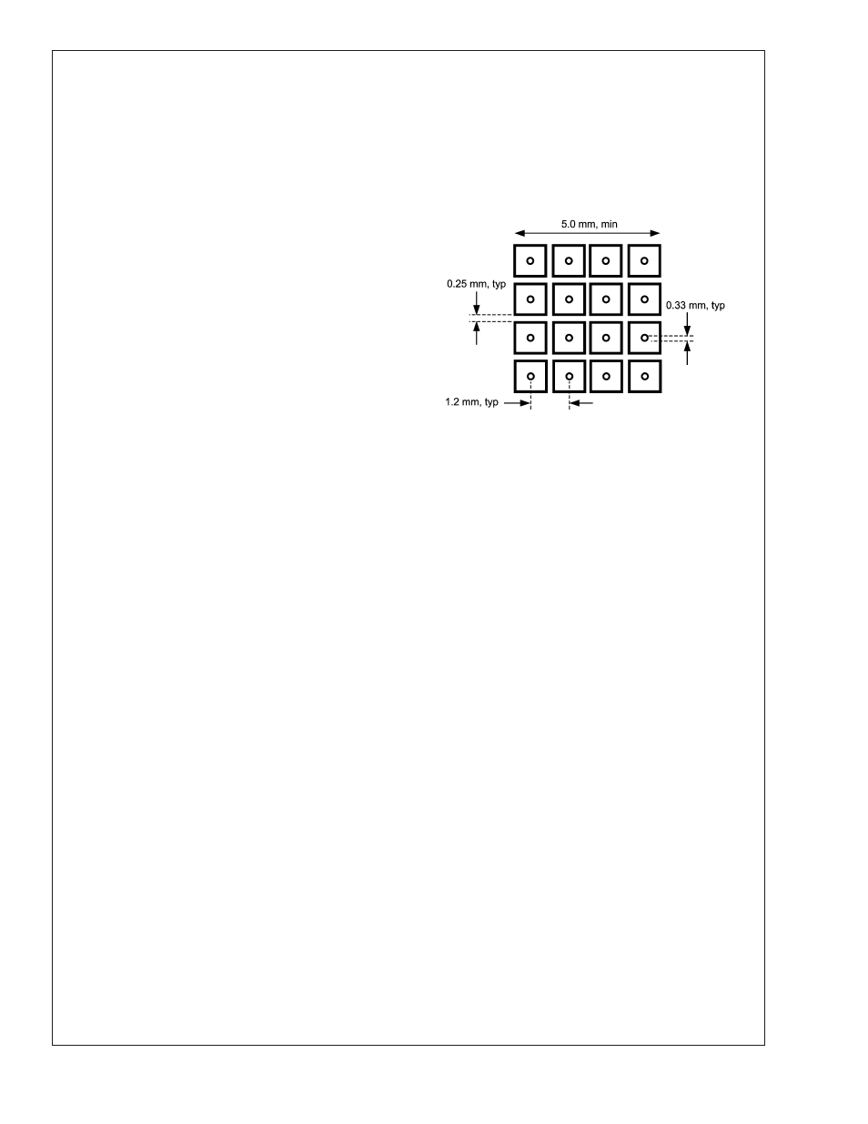
Since a large aperture opening may result in poor release,
the aperture opening should be subdivided into an array of
smaller openings, similar to the land pattern of Figure 9.
To minimize junction temperature, it is recommended that a
simple heat sink be built into the PCB. This is done by
including a minimum copper pad of 2 inches by 2 inches (5.1
cm by 5.1 cm) on the opposite side of the PCB. This copper
area may be plated or solder coated to prevent corrosion,
but should not have a conformal coating, which could pro-
vide some thermal insulation. Thermal vias should be used
to connect these top and bottom copper areas. These ther-
mal vias act as "heat pipes" to carry the thermal energy from
the device side of the board to the opposite side of the board
where it can be more effectively dissipated. The use of 9 to
16 thermal vias is recommended.
The thermal vias should be placed on a 1.2 mm grid spacing
and have a diameter of 0.30 to 0.33 mm. These vias should
be barrel plated to avoid solder wicking into the vias during
the soldering process as this wicking could cause voids in
the solder between the package exposed pad and the ther-
mal land on the PCB. Such voids could increase the thermal
resistance between the device and the thermal land on the
board, which would cause the device to run hotter.
On a board of FR-4 material and the built in heat sink
described above (4 square inch pad and 9 thermal vias), the
die temperature stabilizes at about 30˚C above the ambient
temperature in about 20 seconds.
If it is desired to monitor die temperature, a temperature
sensor may be mounted on the heat sink area of the board
near the thermal vias. Allow for a thermal gradient between
the temperature sensor and the ADC081000 die of
θ
JC
times
typical power consumption = 2.8 x 1.43 = 4˚C. Allowing for a
5˚C (including an extra 1˚C) temperature drop from the die to
the temperature sensor, then, would mean that maintaining a
maximum pad temperature reading of 125˚C will ensure that
the die temperature does not exceed 130˚C, assuming that
the exposed pad of the ADC081000 is properly soldered
down and the thermal vias are adequate.
20068151
FIGURE 9. Recommended Package Land Pattern
ADC081000
www.national.com
27