Pin descriptions and equivalent circuits – Rainbow Electronics ADC081000 User Manual
Page 3
Pin Descriptions and Equivalent Circuits
Pin Functions
Pin No.
Symbol
Equivalent Circuit
Description
3
OutV
Output Voltage Amplitude set. Tie this pin high for
normal differential output amplitude. Ground this pin for
a reduced differential output amplitude and reduced
power consumption. See Section 1.5.
4
OutEdge
Output Edge Select. Sets the edge of the DCLK+ (pin
82) at which the output data transitions. The output
transitions with the DCLK+ rising edge when this pin is
high or on the falling edge when this pin is low. See
Section 5.3.
14
DC_Coup
DC Coupling select. When this pin is high, the V
IN
+ and
V
IN
- analog inputs are d.c. coupled and the input
common mode voltage should equal the V
CMO
(pin 7)
output voltage. When this pin is low, the analog input
pins are internally biased and the input signal should be
a.c. coupled to the analog input pins. See Section 3.0.
26
PD
Power Down Pin. A logic high on this pin puts the ADC
into the Power Down mode. A logic low on this pin
allows normal operation.
30
CAL
Calibration. A minimum 10 clock cycles low followed by
a minimum of 10 clock cycles high on this pin will
initiate the self calibration sequence. See Section 1.1.
35
FSR
Full scale Range Select. With a logic low on this pin,
the full-scale differential input is 600 mV
P-P
. With a logic
high on this pin, the full-scale differential input is 800
mV
P-P
. See Section 1.3.
127
CalDly
Calibration Delay. This sets the number of clock cycles
after power up before calibration begins. See Section
1.1.
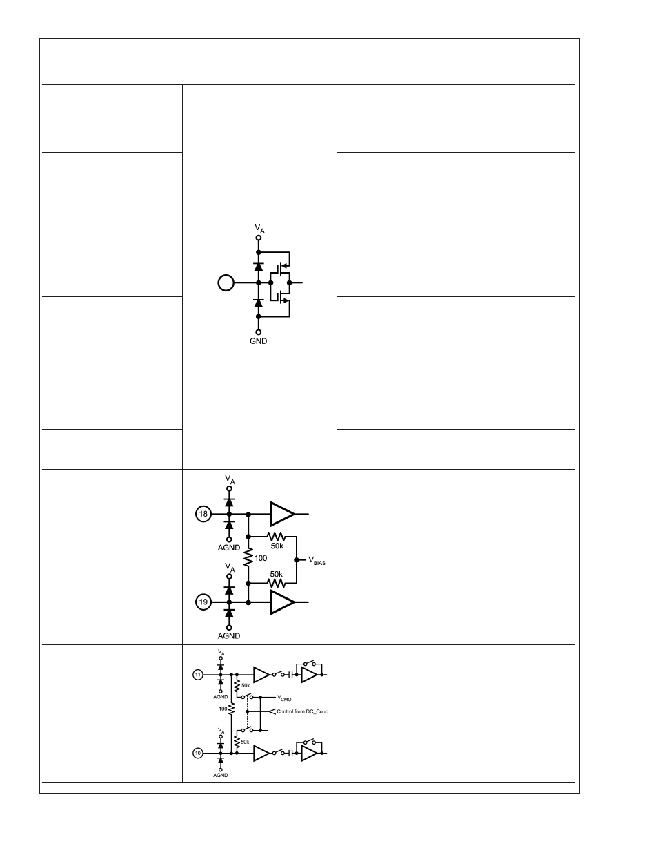
18
19
CLK+
CLK-
Clock input pins for the ADC. The differential clock
signal must be a.c. coupled to these pins. The input
signal is sampled on the falling edge of CLK+.
11
10
V
IN
+
V
IN
-
Analog Signal Differential Inputs to the ADC.
ADC081000
www.national.com
3