Figure 4. differential input drive, 1 handling single-ended analog signals, 2 out of range (or) indication – Rainbow Electronics ADC081000 User Manual
Page 24: 3 full-scale input range, Applications information
Applications Information
(Continued)
TABLE 3. DIFFERENTIAL INPUT TO OUTPUT
RELATIONSHIP (FSR High)
V
IN
+
V
IN
−
Output Code
V
CM
− 200 mV
V
CM
+ 200 mV
0000 0000
V
CM
− 99 mV
V
CM
+ 99 mV
0100 0000
V
CM
V
CM
0111 1111 /
1000 0000
V
CM
+ 101 mV
V
CM
− 101 mV
1100 0000
V
CM
+ 200mV
V
CM
− 200 mV
1111 1111
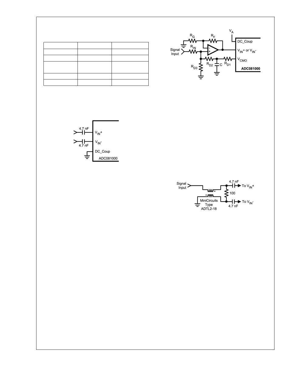
Note that a precise d.c. common mode voltage must be
present at the ADC inputs. This common mode voltage,
V
CMO
, is provided on-chip when DC_Coup (pin 14) is low
and the input signal is a.c. coupled to the ADC through
4.7 nF capacitors. See Figure 4.
When pin 14 is high, the analog inputs are d.c. coupled and
a common mode voltage must be externally provided at the
analog input pins. This common mode voltage should track
the V
CMO
output voltage. Note that the V
CMO
output potential
will change with temperature. The common mode output of
the driving device should track this change. Full-scale dis-
tortion performance falls off rapidly as the input common
mode voltage deviates from V
CMO
. This is a direct result of
using a very low supply voltage to minimize power. Keep the
input common voltage within 50 mV of V
CMO
.
Performance is as good in the d.c. coupled mode as it is in
the a.c. coupled mode, provided the input common mode
voltage at both analog input pins remain within 50 mV of
V
CMO
.
If d.c. coupling is used, it is best to servo the input common
mode voltage, using the V
CMO
pin, to maintain optimum
performance. An example of this type of circuit is shown in
Figure 5. One such circuit should be used in front of the V
IN
+
input and another in front of the V
IN
− input. In that figure,
R
D1
, R
D2
and R
D3
are used to divide the V
CMO
potential so
that, after being gained up by the amplifier, the input com-
mon mode voltage is equal to V
CMO
from the ADC. R
D1
and
R
D2
are split to allow the bypass capacitor to isolate the input
signal from V
CMO
. R
IN
, R
D2
and R
D3
will divide the input
signal, if necessary. Capacitor "C" in Figure 5 should be
chosen to keep any component of the input signal from
affecting V
CMO
.
Be sure that any current drawn from the V
CMO
output does
not exceed
±
1 µA.
The Input impedance in the d.c. coupled mode (DC_Coup
pin high) consists of a precision 100 Ohm resistor between
V
IN
+ and V
IN
- and a capacitance from each of these inputs to
ground. Driving the inputs beyond full scale will result in
saturation or clipping of the reconstructed output.
3.1 Handling Single-Ended Analog Signals
There is no provision for the ADC081000 to adequately
process single-ended input signals. The best way to handle
single-ended signals is to convert them to differential signals
before presenting them to the ADC. The easiest way to
accomplish single-ended to differential signal conversion is
with an appropriate balun-connected transformer, as shown
in Figure 6.
3.2 Out Of Range (OR) Indication
When the conversion result is clipped the Out of Range
output is activated such that OR+ goes high and OR- goes
low. This output is active as long as accurate data on either
or both of the buses would be outside the range of 00h to
FFh.
3.3 Full-Scale Input Range
As with all A/D Converters, the input range is determined by
the value of the ADC’s reference voltage. The reference
voltage of the ADC081000 is derived from an internal band-
gap reference. The FSR pin controls the effective reference
voltage of the ADC081000 such that the differential full-scale
input range at the analog inputs is 800 mV
P-P
with the FSR
pin high, or is 600 mV
P-P
with FSR pin low. Best SNR is
obtained with FSR high, but better distortion and SFDR are
obtained with the FSR pin low.
20068149
FIGURE 4. Differential Input Drive
20068155
FIGURE 5. Example of Servoing the Analog Input with
V
CMO
20068146
FIGURE 6. Single-Ended to Differential signal
conversion with a balun-connected transformer
ADC081000
www.national.com
24