Pin descriptions and equivalent circuits – Rainbow Electronics ADC081000 User Manual
Page 5
Pin Descriptions and Equivalent Circuits
(Continued)
Pin Functions
Pin No.
Symbol
Equivalent Circuit
Description
104
105
106
107
111
112
113
114
115
116
117
118
122
123
124
125
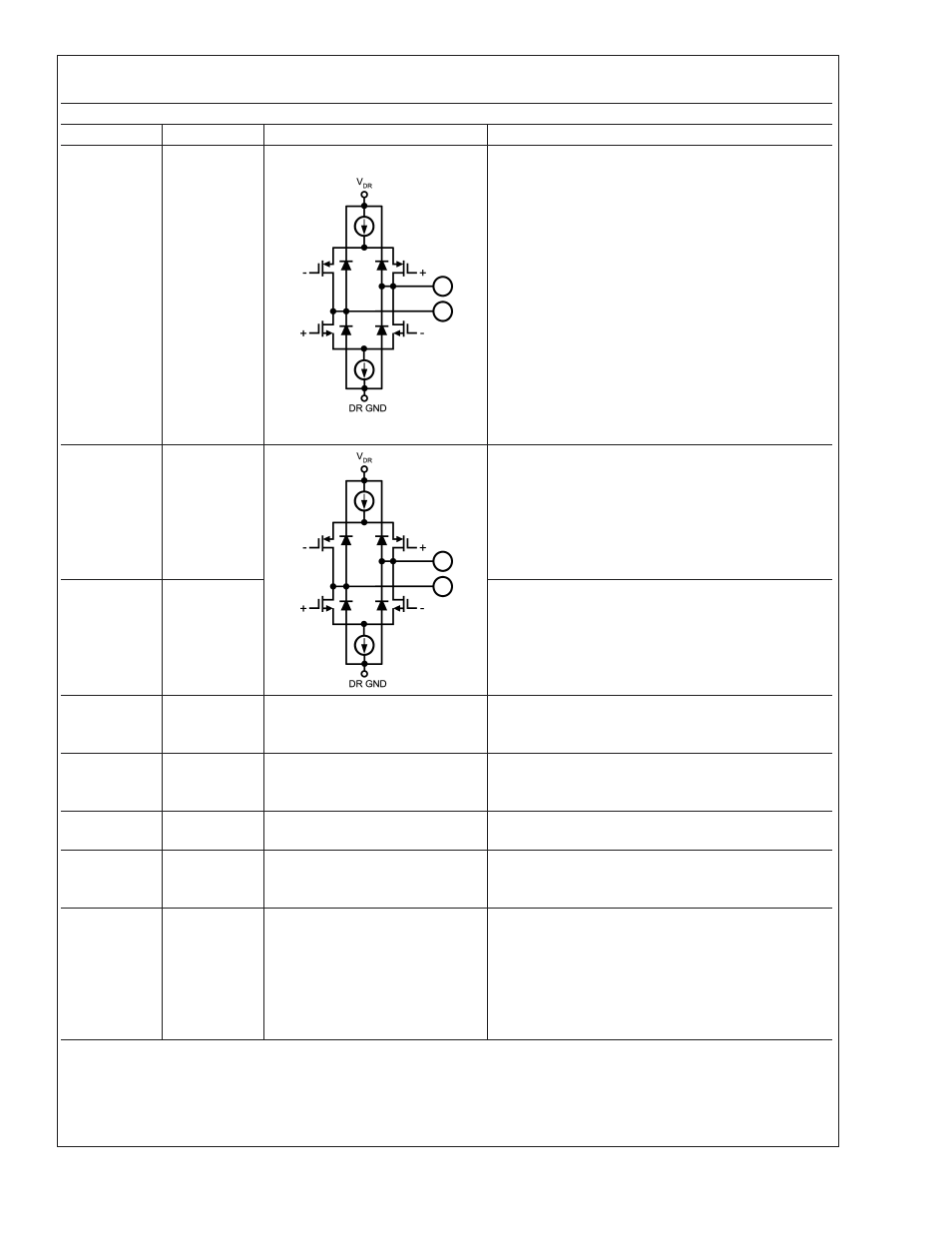
Dd7-
Dd7+
Dd6-
Dd6+
Dd5-
Dd5+
Dd4-
Dd4+
Dd3-
Dd3+
Dd2-
Dd2+
Dd1-
Dd1+
Dd0-
Dd0+
LVDS data output bits sampled first in time sequence.
These outputs should always be terminated with a
differential 100
Ω resistance.
79
80
OR+
OR-
Out of Range output. A differential high at these pins
indicates that the differential input is out of range
(outside the range of
±
300 mV or
±
400 mV as defined
by the FSR pin). See Section 1.6.
82
81
DCLK+
DCLK-
Differential Clock Outputs used to latch the output data.
Delayed and non-delayed data outputs are supplied
synchronous to this signal.
2, 5, 8, 13, 16,
17, 20, 25, 28,
33, 128
V
A
Analog power supply pins. Bypass these pins to GND.
40, 51, 62, 73,
88, 99, 110,
121
V
DR
Output Driver power supply pins. Bypass these pins to
DR GND.
1, 6, 9, 12, 15,
21, 24, 27
GND
Ground return for V
A
42, 53, 64, 74,
87, 97, 108,
119
DR GND
Ground return for V
DR
22, 23, 29, 34,
36 - 39,
41, 43 - 50,
52, 54 - 61,
63, 65 - 72,
75 - 78, 98,
109, 120
NC
No Connection. Make no connection to these pins.
ADC081000
www.national.com
5