3 sleep mode – Rainbow Electronics ATA6631 User Manual
Page 8
8
9165A–AUTO–11/09
ATA6629/ATA6631
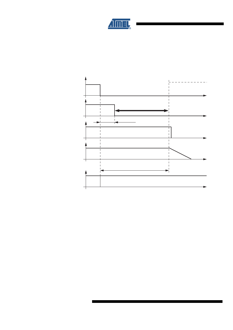
4.3
Sleep Mode
A falling edge at EN while TXD is low switches the IC into Sleep Mode. The TXD Signal has to
be logic low during the Mode Select window (
).
Figure 4-4.
Switch to Sleep Mode
In order to avoid any influence to the LIN-pin during switching into sleep mode it is possible to
switch the EN up to 3.2 µs earlier to Low than the TXD. Therefore, the best an easiest way are
two falling edges at TXD and EN at the same time.
In Sleep Mode the transmission path is disabled. Supply current from V
Batt
is typically
I
VSsleep
= 10 µA. The V
CC
regulator is switched off; NRES and RXD are low. The internal slave
termination between pin LIN and pin VS is disabled to minimize the current consumption in case
pin LIN is short-circuited to GND. Only a weak pull-up current (typically 10 µA) between pin LIN
and pin VS is present. The Sleep Mode can be activated independently from the current level on
pin LIN.
Del
a
y time
s
leep mode
t
d_
s
leep
= m
a
xim
u
m 20
µs
LIN
s
witche
s
directly to rece
ss
ive mode
t
d
=
3
.2
µs
LIN
VCC
NRE
S
TXD
EN
S
leep Mode
Normal Mode
Mode
s
elect window