Electrical characteristics (continued) – Rainbow Electronics ATA6631 User Manual
Page 19
19
9165A–AUTO–11/09
ATA6629/ATA6631
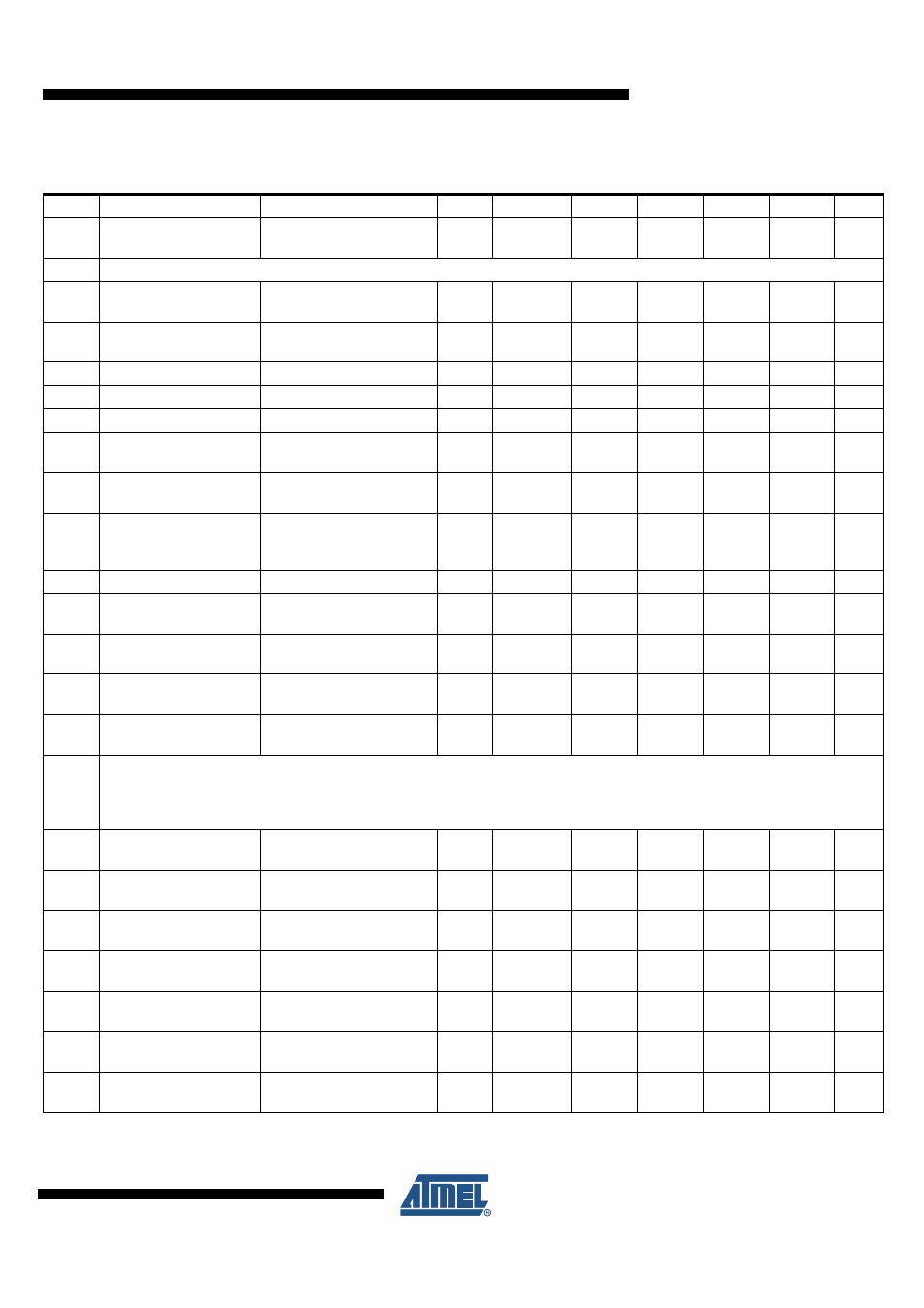
6.12
Ramp up time VS > 4V
to VCC = 3.3V
C
VCC
= 2.2 µF
I
load
= –5 mA at VCC
VCC
t
VCC
100
250
µs
A
7
VCC Voltage Regulator ATA6631
7.1
Output voltage V
CC
5.5V < VS < 18V
(0 mA to 50 mA)
VCC
VCC
nor
4.9
5.1
V
A
7.2
Output voltage V
CC
at
low V
S
4V < VS < 5.5V
VCC
VCC
low
V
VS
– V
D
5.1
V
A
7.3
Regulator drop voltage
VS > 4V, I
VCC
= –20 mA
VCC
V
D1
250
mV
A
7.4
Regulator drop voltage
VS > 4V, I
VCC
= –50 mA
VCC
V
D2
400
600
mV
A
7.5
Regulator drop voltage
VS > 3.3V, I
VCC
= –15 mA
VCC
V
D3
200
mV
A
7.6
Line regulation
maximum
5.5V < VS < 18V
VCC
VCC
line
1
%
A
7.7
Load regulation
maximum
5 mA < I
VCC
< 50 mA
VCC
VCC
load
0.5
2
%
A
7.8
Power supply ripple
rejection
10 Hz to 100 kHz
C
VCC
= 10 µF
VS = 14V, I
VCC
= –15 mA
50
dB
C
7.9
Output current limitation VS > 5.5V
VCC
I
VCCs
–240
–160
mA
A
7.10
Load capacity
0.2
Ω
< ESR < 5
Ω
at
100 kHz
VCC
C
load
1.8
10
µF
D
7.11
VCC undervoltage
threshold
Referred to VCC
VS > 5.5V
VCC
V
thunN
4.2
4.8
V
A
7.12
Hysteresis of
undervoltage threshold
Referred to VCC
VS > 5.5V
VCC
Vhys
thun
250
mV
A
7.13
Ramp up time VS > 5.5V
to VCC = 5V
C
VCC
= 2.2 µF
I
load
= –5 mA at VCC
VCC
T
VCC
130
300
µs
A
8
LIN Bus Driver: Bus Load Conditions:
Load 1 (Small): 1 nF, 1 k
Ω
; Load 2 (Large): 10 nF, 500
Ω
; Internal Pull-up R
RXD
= 5 k
Ω
; C
RXD
= 20 pF, Load 3 (Medium): 6.8
nF, 660
Ω
characterized on samples
10.7 and 10.8 Specifies the Timing Parameters for Proper Operation at 20 kBit/s and 10.9 and 10.10 at 10,4 kBit/s
8.1
Driver recessive output
voltage
Load1/Load2
LIN
V
BUSrec
0.9
×
V
S
V
S
V
A
8.2
Driver dominant voltage
V
VS
= 7V
R
load
= 500
Ω
LIN
V
_LoSUP
1.2
V
A
8.3
Driver dominant voltage
V
VS
= 18V
R
load
= 500
Ω
LIN
V
_HiSUP
2
V
A
8.4
Driver dominant voltage
V
VS
= 7V
R
load
= 1000
Ω
LIN
V
_LoSUP_1k
0.6
V
A
8.5
Driver dominant voltage
V
VS
= 18V
R
load
= 1000
Ω
LIN
V
_HiSUP_1k
0.8
V
A
8.6
Pull–up resistor to V
S
The serial diode is
mandatory
LIN
R
LIN
20
30
47
k
Ω
A
8.7
Voltage drop at the serial
diodes
In pull-up path with R
slave
I
SerDiode
= 10 mA
LIN
V
SerDiode
0.4
1.0
V
D
9.
Electrical Characteristics (Continued)
5V < V
S
< 27V, –40°C < T
j
< 150°C; unless otherwise specified all values refer to GND pins.
No.
Parameters
Test Conditions
Pin
Symbol
Min.
Typ.
Max.
Unit
Type*
*) Type means: A = 100% tested, B = 100% correlation tested, C = Characterized on samples, D = Design parameter