Port d, Port d data register – portd, Port d data direction register – ddrd – Rainbow Electronics AT90S1200 User Manual
Page 34: Port d input pins address – pind, Port d as general digital i/o
34
AT90S1200
0838H–AVR–03/02
Port D
Three I/O memory address locations are allocated for Port D, one each for the Data
Register – PORTD ($12), Data Direction Register – DDRD ($11), and the Port D Input
Pins – PIND ($10). The Port D Input Pins address is read-only, while the Data Register
and the Data Direction Register are read/write.
Port D has seven bi-directional I/O pins with internal pull-up resistors, PD6..PD0. The
Port D output buffers can sink 20 mA. As inputs, Port D pins that are externally pulled
low will source current if the pull-up resistors are activated.
Some Port D pins have alternate functions as shown in Table 10.
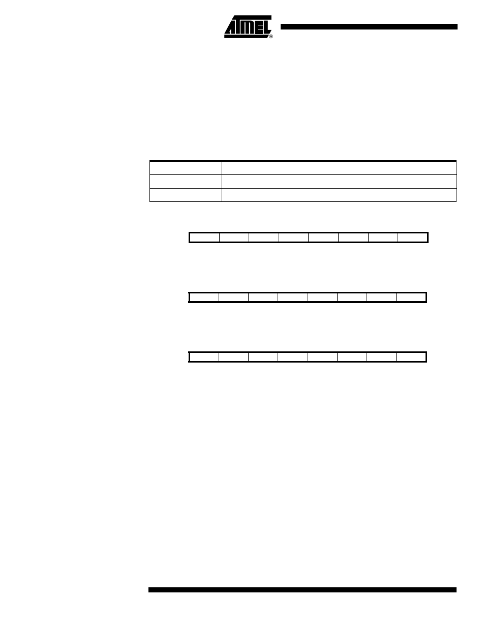
Port D Data Register – PORTD
Port D Data Direction Register
– DDRD
Port D Input Pins Address –
PIND
The Port D Input Pins address (PIND) is not a register, and this address enables access
to the physical value on each Port D pin. When reading PORTD, the Port D Data Latch
is read; and when reading PIND, the logical values present on the pins are read.
Port D as General Digital I/O
PDn, general I/O pin: The DDDn bit in the DDRD Register selects the direction of this
pin. If DDDn is set (one), PDn is configured as an output pin. If DDDn is cleared (zero),
PDn is configured as an input pin. If PORTDn is set (one) when DDDn is configured as
an input pin, the MOS pull-up resistor is activated. To switch the pull-up resistor off, the
PORTDn bit has to be cleared (zero) or the pin has to be configured as an output pin.
The Port D pins are tri-stated when a reset condition becomes active, even if the clock is
not active.
Table 10. Port D Pin Alternate Functions
Port Pin
Alternate Function
PD2
INT0 (External Interrupt 0 input)
PD4
T0 (Timer/Counter 0 external input)
Bit
7
6
5
4
3
2
1
0
$12
–
PORTD6
PORTD5
PORTD4
PORTD3
PORTD2
PORTD1
PORTD0
PORTD
Read/Write
R
R/W
R/W
R/W
R/W
R/W
R/W
R/W
Initial Value
0
0
0
0
0
0
0
0
Bit
7
6
5
4
3
2
1
0
$11
–
DDD6
DDD5
DDD4
DDD3
DDD2
DDD1
DDD0
DDRD
Read/Write
R
R/W
R/W
R/W
R/W
R/W
R/W
R/W
Initial Value
0
0
0
0
0
0
0
0
Bit
7
6
5
4
3
2
1
0
$10
–
PIND6
PIND5
PIND4
PIND3
PIND2
PIND1
PIND0
PIND
Read/Write
R
R
R
R
R
R
R
R
Initial Value
0
N/A
N/A
N/A
N/A
N/A
N/A
N/A