2 schematic, Qt1040 – Rainbow Electronics AT42QT1040 User Manual
Page 3
3
9524A–AT42–03/09
AT42QT1040
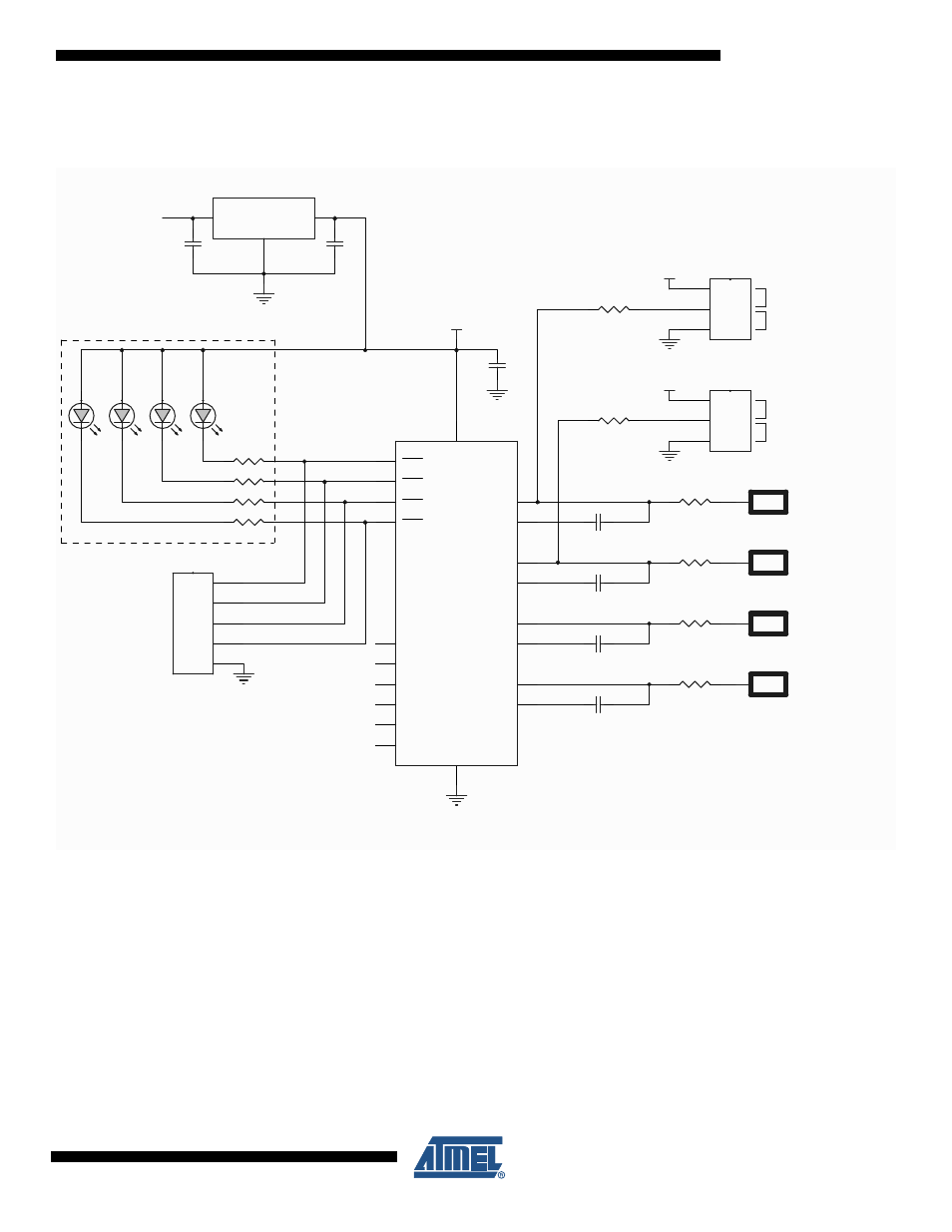
1.2
Schematic
Figure 1-1.
Typical Circuit
Suggested regulator manufacturers:
• Torex (XC6215 series)
• Seiko (S817 series)
• BCDSemi (AP2121 series)
Re
check the following sections for component values:
•
Cs capacitors (Cs0 – Cs3)
•
: Voltage levels
•
: LED traces
SLOW
FAST
OFF
LED3
LED2
LED0
LED1
VDD
VDD
2
1
3
J2
VDD
2
1
3
J1
ON
2
2
5
5
4
4
3
3
1
1
J3
VDD
9
VSS
8
N/C
19
N/C
10
OUT2
14
SNSK3
15
SNSK2
20
SNSK1
2
SNSK0
4
N/C
18
N/C
7
N/C
17
OUT1
12
OUT0
11
SNS3
16
SNS1
3
N/C
6
OUT3
13
SNS0
5
SNS2
1
SPEED SELECT
AKS SELECT
NOTES:
1) The central pad on the underside of the VQFN chip is a Vss pin and should be connected
to ground. Do not put any other tracks underneath the body of the chip.
2) It is important to place all Cs and Rs components physically near to the chip.
Add a 100 nF capacitor close to pin 9.
QT1040
Creg
Creg
VREG
Follow regulator manufacturer's
recommended values for input
and output bypass capacitors (Creg).
Key0
Key1
Key2
Key3
VUNREG
GND
Cs0
Cs1
Cs2
Cs3
RL0
RL1
RL2
RL3
RAKS
RFS
Rs0
Rs1
Rs2
Rs3
Example use of output pins