Pinout and schematic, 1 pinout configuration – Rainbow Electronics AT42QT1040 User Manual
Page 2
2
9524A–AT42–03/09
AT42QT1040
1.
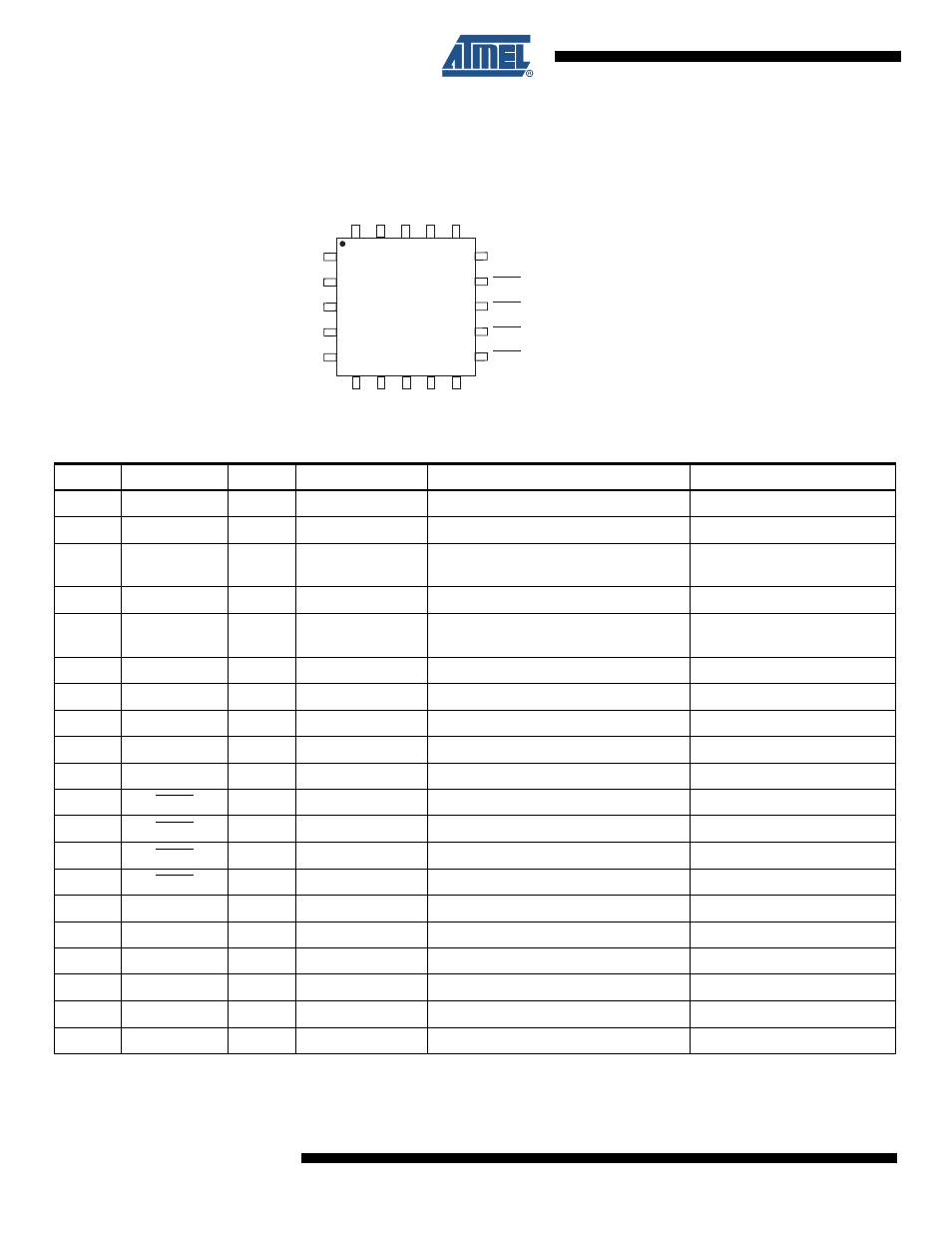
Pinout and Schematic
1.1
Pinout Configuration
I/O
CMOS input and output
OD
CMOS open drain output
P
Ground or power
Table 1-1.
Pin Listing
Pin
Name
Type
Function
Notes
If Unused...
1
SNS2
I/O
Sense pin
To Cs2
Leave open
2
SNSK1
I/O
Sense pin
To Cs1 + key
Leave open
3
SNS1
I/O
Sense pin and
option detect
To Cs1 and/or option resistor
Connect to option resistor*
4
SNSK0
I/O
Sense pin
To Cs0 + key
Leave open
5
SNS0
I/O
Sense pin and
option detect
To Cs0 and/or option resistor
Connect to option resistor*
6
N/C
–
–
–
7
N/C
–
–
–
8
Vss
P
Supply ground
–
9
Vdd
P
Power
–
10
N/C
–
–
–
11
OUT0
OD
Out 0
Alternative function: Debug CLK
Leave open
12
OUT1
OD
Out 1
Alternative function: Debug DATA
Leave open
13
OUT3
OD
Out 3
Leave open
14
OUT2
OD
Out 2
Leave open
15
SNSK3
I/O
Sense pin
To Cs3 + key
Leave open
16
SNS3
I/O
Sense pin
To Cs3
Leave open
17
N/C
–
–
–
18
N/C
–
–
–
19
N/C
–
–
–
20
SNSK2
I/O
Sense pin
To Cs2 + key
Leave open
* Option resistor should always be fitted even if channel is unused and Cs capacitor is not fixed.
N/C
N/C
VSS
VDD
N/C
SNS2
SNSK1
SNS1
SNSK0
SNS0
OUT0
OUT1
1
2
3
4
5
11
12
13
14
15
20 19
18 17
16
6
7
8
10
9
QT1040
OUT3
OUT2
SNSK3
SNS3
N/C
SNSK2
N/C
N/C