Ata6830, Digital blocks – Rainbow Electronics ATA6830 User Manual
Page 5
5
ATA6830
4575B–BCD–01/03
Digital Blocks
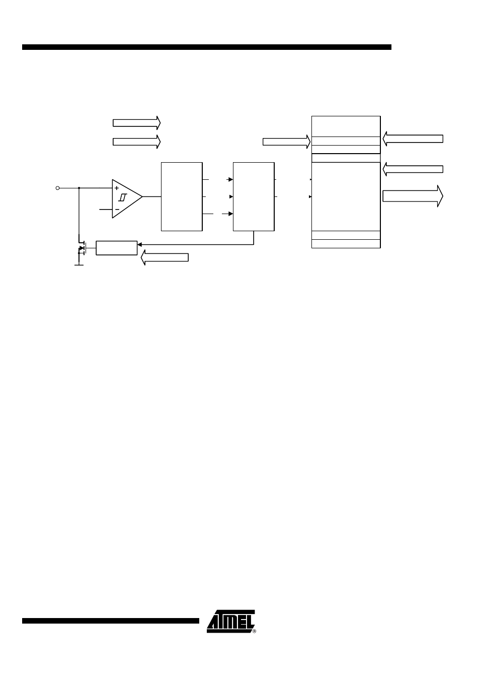
Figure 4.
Digital Blocks
Figure 4 shows all digital blocks of the circuit. The stepping motor will be controlled by
commands via the bus input pin. An analog comparator is used as a level shifter at the
input. There is also a possibility of clamping the bus pin to ground. This will be used after
detecting an error to feedback this to the microcontroller.
The next block is a UART. Its task is clock recovery and data recognition of the incoming
bit stream. For clock recovery a special bitstream is used after each power on. The gen-
erated bitstream will be analyzed and after a correct parity check interpreted for
execution.
A sophisticated cruise control generates all control signals for the two H-bridge drivers.
It uses an internal step-time table for accelerating and decelerating the stepping motor
depending on the actual and desired position and the temperature and voltage levels.
Exception handling is integrated to interpret and react on the temperature, supply volt-
age, and coil-current signals from the analog part.
UART
Clock
Recovery
Bitstream
Recovery
Data
Recognition
&
Parity-Check
bitstream
rxd
shiftclk
BUS
VREF
reference run
new position
Step Time Memory
Maximum Step Time
New Step Time
Clk
Voltage Levels
Actual Step Time
Cruise Control
Desired Position
Instantaneous Position
Stepper Motor Control
Error Timer
Error Signals
Temperature Signals
Error Signals
Reset