Low-current i, Ac electrical characteristics, Crystal parameters – Rainbow Electronics DS1342 User Manual
Page 3
Low-Current I
2
C RTCs for High-ESR Crystals
DS1341/DS1342
3
AC ELECTRICAL CHARACTERISTICS
(V
CC
= +1.8V to +5.5V, T
A
= -40NC to +85NC, unless otherwise noted.) (Note 2, Figure 1)
CRYSTAL PARAMETERS
Note 2: Limits at -40NC are guaranteed by design and not production tested.
Note 3: Voltage referenced to ground.
Note 4: Specified with I
2
C bus inactive. Oscillator operational, INTCN = 1, ECLK = 0.
Note 5: Applies to CLKIN/INTA and SQW/INTB only.
Note 6: The minimum SCL clock frequency is limited by the bus timeout feature, which resets the serial bus interface if SCL is
held low for t
TIMEOUT
.
Note 7: After this period, the first clock pulse is generated.
Note 8: A device must internally provide a hold time of at least 300ns for the SDA signal (referred to the V
IHMIN
of the SCL sig-
nal) to bridge the undefined region of the falling edge of SCL.
Note 9: The maximum t
HD:DAT
need only be met if the device does not stretch the low period (t
LOW
) of the SCL signal.
Note 10: A fast-mode device can be used in a standard-mode system, but the requirement t
SU:DAT
R to 250ns must then be
met. This is automatically the case if the device does not stretch the low period of the SCL signal. If such a device does
stretch the low period of the SCL signal, it must output the next data bit to the SDA line t
RMAX
+ t
SU:DAT
= 1000 + 250 =
1250ns before the SCL line is released.
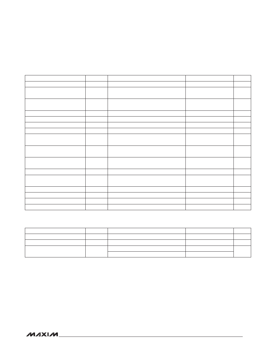
PARAMETER
SYMBOL
CONDITIONS
MIN
TYP
MAX
UNITS
SCL Clock Frequency
f
SCL
(Note 6)
400
kHz
Bus Free Time Between a STOP
and START Condition
t
BUF
1.3
F
s
Hold Time (Repeated) START
Condition
t
HD:STA
(Note 7)
0.6
F
s
Low Period of SCL Clock
t
LOW
1.3
F
s
High Period of SCL Clock
t
HIGH
0.6
F
s
Data Hold Time
t
HD:DAT
(Notes 8, 9)
0
0.9
F
s
Data Setup Time
t
SU:DAT
(Note 10)
100
ns
Setup Time for a Repeated
START Condition
t
SU:STA
0.6
F
s
Rise Time of Both SDA and SCL
Signals
t
R
(Note 11)
20 +
0.1C
B
300
ns
Fall Time for Both SDA and SCL
Signals
t
F
(Note 11)
20 +
0.1C
B
300
ns
Setup Time for STOP Condition
t
SU:STO
0.6
F
s
Capacitive Load for Each Bus
Line
C
B
(Note 11)
400
pF
I/O Capacitance
C
I/O
10
pF
SCL Spike Suppression
t
SP
30
ns
Oscillator Stop Flag (OSF) Delay
t
OSF
(Note 12)
25
100
ms
Timeout Interval
t
TIMEOUT
(Note 13)
25
35
ms
PARAMETER
SYMBOL
CONDITIONS
MIN
TYP
MAX
UNITS
Nominal Frequency
f
O
32.768
kHz
Series Resistance
ESR
35
80
kI
Load Capacitance
C
L
DS1341
6
pF
DS1342
12.5