Low-current i – Rainbow Electronics DS1342 User Manual
Page 10
Low-Current I
2
C RTCs for High-ESR Crystals
DS1341/DS1342
10
of a match with date of the month. If DY/DT is written to
1, the alarm is the result of a match with day of the week.
When the RTC register values match alarm register set-
tings, the corresponding alarm flag bit (A1F or A2F) is
set to 1 in the Control/Status register. If the correspond-
ing alarm interrupt enable bit (A1IE or A2IE) is also set
to 1 in the Control register, the alarm condition activates
the output(s) defined by the ECLK and INTCN bits (see
Table 5).
Control Register (0Eh)
Bit 7: Enable Oscillator (EOSC). When the EOSC bit
is 0, the oscillator is enabled. When this bit is a 1, the
oscillator is disabled. This bit is cleared (0) when power
is first applied.
Bit 6: No Function
Bit 5: Enable Glitch Filter (EGFIL). When the EGFIL bit
is 1, the 5Fs glitch filter at the output of the crystal oscil-
lator is enabled. The glitch filter is disabled when this bit
is 0. Disabling the glitch filter is useful in reducing power
consumption. This bit is cleared (0) when power is first
applied.
Bits 4 and 3: Rate Select (RS[2:1]). These bits con-
trol the frequency of the square-wave output when the
square wave has been enabled. Table 4 shows the
square-wave frequencies that can be selected with the
RS bits. These bits are both set to 1 (32.768kHz) when
power is first applied.
The 32.768kHz oscillator is the source of all square-wave
output frequencies. Frequencies above 1Hz are not con-
ditioned by CLKIN. The 1Hz output is the 32.768kHz oscil-
lator frequency, divided down to 1Hz and conditioned by
CLKIN, provided that the CLKIN frequency differs by no
more than Q0.8% from the crystal frequency. Cycle-to-
cycle jitter of the 1Hz square wave can be up to 2ms.
Bit 2: Interrupt Control (INTCN). This bit controls the
relationship between the two alarms and the interrupt
output pins. When the INTCN bit is 0, a square wave is
output on the SQW/INTB pin, and the state of the ECLK
bit determines the function of the CLKIN/INTA pin (see
Table 5). When the INTCN bit is 1 and the ECLK bit is a
0, a match between the timekeeping registers and the
alarm 1 registers activates the CLKIN/INTA pin (provided
that the alarm is enabled) and a match between the
timekeeping registers and the alarm 2 registers activates
the SQW/INTB pin (provided that the alarm is enabled).
When the INTCN bit is 1 and the ECLK bit is a 1, a match
between the timekeeping registers and the alarm 1
registers or a match between the timekeeping registers
and the alarm 2 registers activates the SQW/INTB pin
(provided that the alarm is enabled). This bit is cleared
(0) when power is first applied.
Bit 1: Alarm 2 Interrupt Enable (A2IE). When the A2IE
bit is 0, the alarm 2 interrupt function is disabled. When
the A2IE bit is 1, the alarm 2 interrupt function is enabled
and is routed to an output, based upon the steering
defined by the INTCN and ECLK bits, as noted in Table
5. Regardless of the state of A2IE, a match between
the timekeeping registers and the alarm 2 registers
(0Bh–0Dh) sets the alarm 2 flag bit (A2F). This bit is
cleared (0) when power is first applied.
Bit 0: Alarm 1 Interrupt Enable (A1IE). When the A1IE
bit is 0, the alarm 1 interrupt function is disabled. When
the A1IE bit is 1, the alarm 1 interrupt function is enabled
and is routed to an output, based upon the steering
defined by the INTCN and ECLK bits, as noted in Table
5. Regardless of the state of A1IE, a match between the
timekeeping registers and the alarm 1 registers (07h–
0Ah) sets the alarm 1 flag bit (A1F). This bit is cleared (0)
when power is first applied.
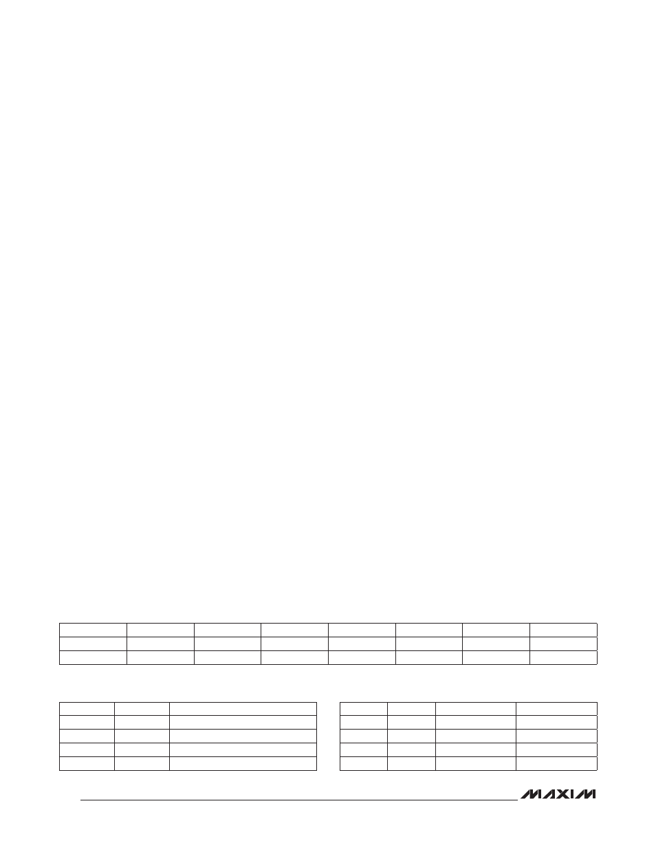
Control Register Bitmap (0Eh)
Table 4. SQW/INTB Output Settings
Table 5. Interrupt Output Routing
BIT 7
BIT 6
BIT 5
BIT 4
BIT 3
BIT 2
BIT 1
BIT 0
EOSC
0
EGFIL
RS2
RS1
INTCN
A2IE
A1IE
0
0
0
1
1
0
0
0
RS2
RS1
SQW/INTB
0
0
1Hz
0
1
4.098kHz
1
0
8.192kHz
1
1
32.768kHz
INTCN
ECLK
CLKIN/INTA
SQW/INTB
0
0
A1F + A2F
SQW
0
1
CLKIN Input
SQW
1
0
A1F
A2F
1
1
CLKIN Input
A1F + A2F