Low-current i, Dc electrical characteristics, Absolute maximum ratings – Rainbow Electronics DS1342 User Manual
Page 2
Low-Current I
2
C RTCs for High-ESR Crystals
DS1341/DS1342
2
Stresses beyond those listed under “Absolute Maximum Ratings” may cause permanent damage to the device. These are stress ratings only, and functional
operation of the device at these or any other conditions beyond those indicated in the operational sections of the specifications is not implied. Exposure to absolute
maximum rating conditions for extended periods may affect device reliability.
Voltage Range on Any Pin Relative to Ground ....-0.3V to +6.0V
Operating Temperature Range .......................... -40NC to +85NC
Junction-to-Ambient Thermal
Resistance (B
JA
) (Note 1) ........................................ +221NC/W
Junction-to-Case Thermal
Resistance (B
JC
) (Note 1) ......................................... +39NC/W
Junction Temperature Maximum .....................................+150NC
Storage Temperature Range ............................ -55NC to +125NC
Soldering Temperature .........................Refer to the IPC/JEDEC
J-STD-020 Specification.
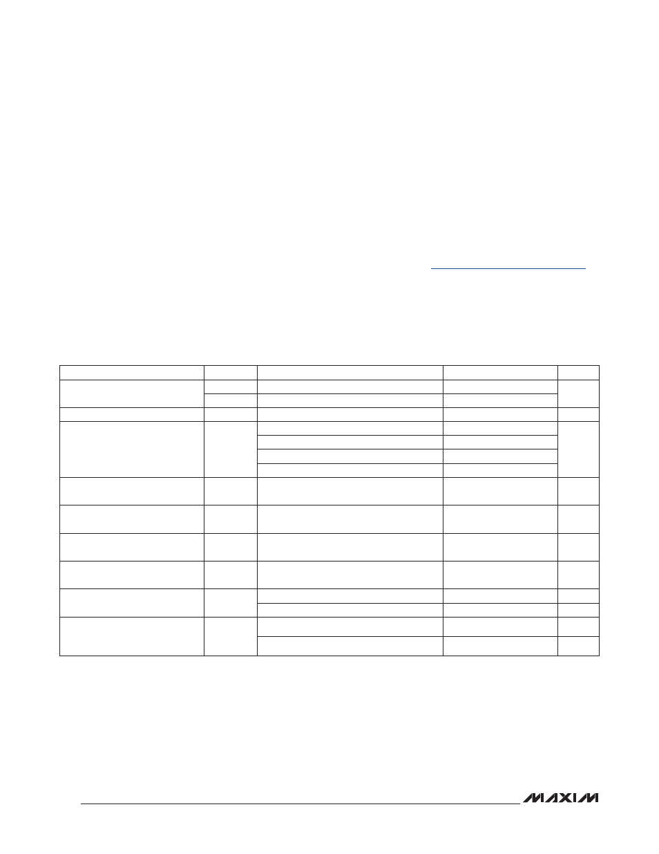
DC ELECTRICAL CHARACTERISTICS
(V
CC
= +1.8V to +5.5V, T
A
= -40NC to +85NC, unless otherwise noted.) (Note 2)
ABSOLUTE MAXIMUM RATINGS
Note 1: Package thermal resistances were obtained using the method described in JEDEC specification JESD51-7, using a four-
layer board. For detailed information on package thermal considerations, refer to
.
PARAMETER
SYMBOL
CONDITIONS
MIN
TYP
MAX
UNITS
Operating Voltage Range
V
CC
Full operation (Note 3)
1.8
5.5
V
V
CCT
Timekeeping (Notes 3, 4)
1.3
5.5
Minimum Timekeeping Voltage
V
CCTMIN
T
A
= +25NC (Notes 3, 4)
1.15
1.3
V
Timekeeping Current: DS1341
CLKIN = GND or CLKIN = V
CC
(Note 4)
I
CCT
V
CC
= +3.0V, EGFIL = 0, DOSF = 1
220
500
nA
V
CC
= +5.5V
250
600
V
CC
= +3.0V, EGFIL = 1, DOSF = 0
280
560
V
CC
= +5.5V
320
700
Logic 1 Input
V
IH
(Note 2)
0.7 x
V
CC
V
CC
+
0.3
V
Logic 0 Input
V
IL
(Note 2)
-0.3
0.3 x
V
CC
V
Input Leakage
(SCL, CLKIN/INTA)
I
LI
ECLK = 1, V
IN
= 0V to V
CC
-0.1
+0.1
F
A
Output Leakage
(CLKIN/INTA, SQW/INTB)
I
O
ECLK = A1IE = A2IE = 0
-1.0
+1.0
F
A
Output Logic 1
V
OH
= +1.0V (SQW /INTB)
I
OH
V
CC
R 1.8V, INTCN = 0
-3.0
mA
V
CC
R 1.3V, INTCN = 0
-250
F
A
Output Logic 0
V
OL
= +0.4V (SDA, CLKIN/INTA,
SQW/INTB)
I
OL
V
CC
R 1.8V
3.0
mA
V
CC
R 1.3V (Note 5)
250
F
A