Enter programming mode, Chip erase – Rainbow Electronics AT90S2313 User Manual
Page 62
62
AT90S2313
0839I–AVR–06/02
Enter Programming Mode
The following algorithm puts the device in Parallel Programming mode:
1.
Apply supply voltage according to Table 22, between V
CC
and GND.
2.
Set the RESET and BS pin to “0” and wait at least 100 ns.
3.
Apply 11.5 - 12.5V to RESET. Any activity on BS within 100 ns after +12V has
been applied to RESET, will cause the device to fail entering Programming
mode.
Chip Erase
The Chip Erase command will erase the Flash and EEPROM memories, and the Lock
bits. The Lock bits are not reset until the Flash and EEPROM have been completely
erased. The Fuse bits are not changed. Chip Erase must be performed before the Flash
or EEPROM is reprogrammed.
Load Command “Chip Erase”
1.
Set XA1, XA0 to “10”. This enables command loading.
2.
Set BS to “0”.
3.
Set DATA to “1000 0000”. This is the command for Chip Erase.
4.
Give XTAL1 a positive pulse. This loads the command.
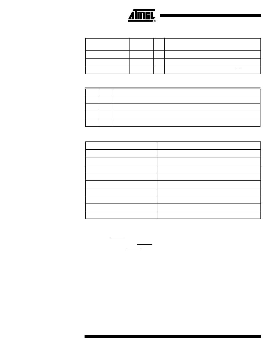
XA0
PD5
I
XTAL Action Bit 0
XA1
PD6
I
XTAL Action Bit 1
DATA
PB7 - 0
I/O
Bi-directional Data Bus (Output when OE is low)
Table 24. XA1 and XA0 Coding
XA1
XA0
Action when XTAL1 is Pulsed
0
0
Load Flash or EEPROM Address (High or low address byte determined by BS)
0
1
Load Data (High or Low data byte for Flash determined by BS)
1
0
Load Command
1
1
No Action, Idle
Table 25. Command Byte Bit Coding
Command Byte
Command Executed
1000 0000
Chip Erase
0100 0000
Write Fuse Bits
0010 0000
Write Lock Bits
0001 0000
Write Flash
0001 0001
Write EEPROM
0000 1000
Read Signature Bytes
0000 0100
Read Fuse and Lock Bits
0000 0010
Read Flash
0000 0011
Read EEPROM
Table 23. Pin Name Mapping
Signal Name in
Programming Mode
Pin Name
I/O
Function