Status register – sreg – Rainbow Electronics AT90S2313 User Manual
Page 16
16
AT90S2313
0839I–AVR–06/02
Note:
1. Reserved and unused locations are not shown in the table.
All AT90S2313 I/O and peripherals are placed in the I/O space. The I/O locations are
accessed by the IN and OUT instructions transferring data between the 32 general pur-
pose working registers and the I/O space. I/O Registers within the address range $00 -
$1F are directly bit-accessible using the SBI and CBI instructions. In these registers, the
value of single bits can be checked by using the SBIS and SBIC instructions. Refer to
the instruction set section for more details. When using the I/O specific commands IN
and OUT, the I/O addresses $00 - $3F must be used. When addressing I/O Registers as
SRAM, $20 must be added to this address. All I/O Register addresses throughout this
document are shown with the SRAM address in parentheses.
For compatibility with future devices, reserved bits should be written to zero if accessed.
Reserved I/O memory addresses should never be written.
Some of the Status Flags are cleared by writing a logical “1” to them. Note that the CBI
and SBI instructions will operate on all bits in the I/O Register, writing a “1” back into any
flag read as set, thus clearing the flag. The CBI and SBI instructions work with registers
$00 to $1F only.
The I/O and peripherals control registers are explained in the following sections.
Status Register – SREG
The AVR Status Register (SREG) at I/O space location $3F ($5F) is defined as:
• Bit 7 – I: Global Interrupt Enable
The Global Interrupt Enable bit must be set (one) for the interrupts to be enabled. The
individual interrupt enable control is then performed in separate control registers. If the
Global Interrupt Enable bit is cleared (zero), none of the interrupts are enabled indepen-
dent of the individual interrupt enable settings. The I-bit is cleared by hardware after an
interrupt has occurred, and is set by the RETI instruction to enable subsequent
interrupts.
• Bit 6 – T: Bit Copy Storage
The Bit Copy instructions BLD (Bit LoaD) and BST (Bit STore) use the T-bit as source
and destination for the operated bit. A bit from a register in the Register File can be cop-
ied into T by the BST instruction, and a bit in T can be copied into a bit in a register in the
Register File by the BLD instruction.
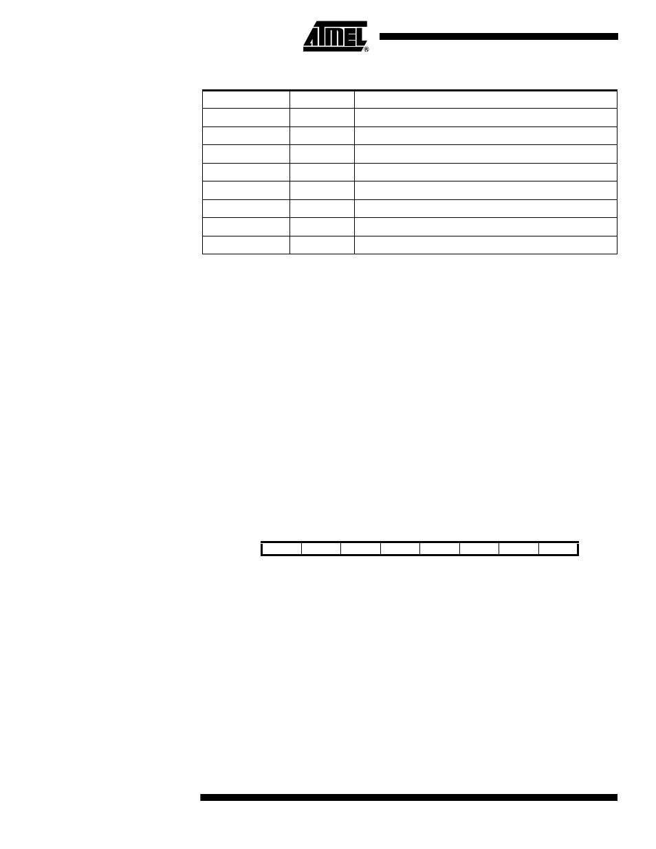
$12 ($32)
PORTD
Data Register, Port D
$11 ($31)
DDRD
Data Direction Register, Port D
$10 ($30)
PIND
Input Pins, Port D
$0C ($2C)
UDR
UART I/O Data Register
$0B ($2B)
USR
UART Status Register
$0A ($2A)
UCR
UART Control Register
$09 ($29)
UBRR
UART Baud Rate Register
$08 ($28)
ACSR
Analog Comparator Control and Status Register
Table 1. AT90S2313 I/O Space
(1)
(Continued)
Address Hex
Name
Function
Bit
7
6
5
4
3
2
1
0
$3F ($5F)
I
T
H
S
V
N
Z
C
SREG
Read/Write
R/W
R/W
R/W
R/W
R/W
R/W
R/W
R/W
Initial value
0
0
0
0
0
0
0
0