Memory access and instruction execution timing – Rainbow Electronics AT90S2313 User Manual
Page 14
14
AT90S2313
0839I–AVR–06/02
Memory Access and
Instruction Execution
Timing
This section describes the general access timing concepts for instruction execution and
internal memory access.
The AVR CPU is driven by the System Clock Ø, directly generated from the external
clock crystal for the chip. No internal clock division is used.
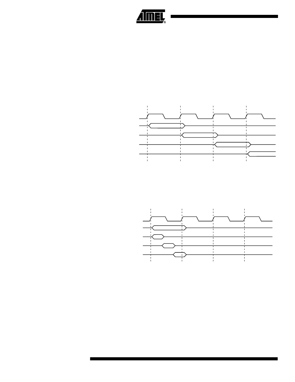
Figure 20 shows the parallel instruction fetches and instruction executions enabled by
the Harvard architecture and the fast-access Register File concept. This is the basic
pipelining concept to obtain up to 1 MIPS per MHz with the corresponding unique results
for functions per cost, functions per clocks and functions per power-unit.
Figure 20. The Parallel Instruction Fetches and Instruction Executions
Figure 21 shows the internal timing concept for the Register File. In a single clock cycle
an ALU operation using two register operands is executed, and the result is stored back
to the destination register.
Figure 21. Single-cycle ALU Operation
The internal data SRAM access is performed in two System Clock cycles as described
in Figure 22.
System Clock Ø
1st Instruction Fetch
1st Instruction Execute
2nd Instruction Fetch
2nd Instruction Execute
3rd Instruction Fetch
3rd Instruction Execute
4th Instruction Fetch
T1
T2
T3
T4
System Clock Ø
Total Execution Time
Register Operands Fetch
ALU Operation Execute
Result Write Back
T1
T2
T3
T4