Port d schematics – Rainbow Electronics AT90S2313 User Manual
Page 57
57
AT90S2313
0839I–AVR–06/02
• INT1 – Port D, Bit 3
INT1, External Interrupt Source 1. The PD3 pin can serve as an external interrupt
source to the MCU. See the interrupt description for further details and how to enable
the source.
• INT0 – Port D, Bit 2
INT0, External Interrupt Source 0. The PD2 pin can serve as an external interrupt
source to the MCU. See the interrupt description for further details and how to enable
the source.
• TXD – Port D, Bit 1
Transmit Data (Data Output pin for the UART). When the UART Transmitter is enabled,
this pin is configured as an output regardless of the value of DDRD1.
• RXD – Port D, Bit 0
Receive Data (Data Input pin for the UART). When the UART Receiver is enabled, this
pin is configured as an input regardless of the value of DDRD0. When the UART forces
this pin to be an input, a logical “1” in PORTD0 will turn on the internal pull-up.
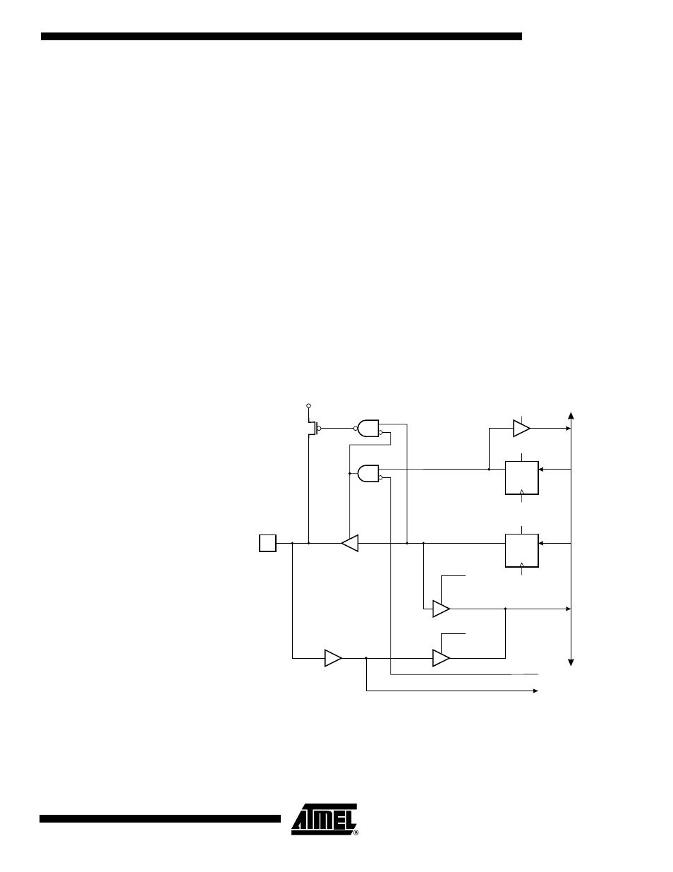
Port D Schematics
Note that all port pins are synchronized. The synchronization latches are, however, not
shown in the figures.
Figure 44. Port D Schematic Diagram (Pin PD0)
DA
T
A
BUS
D
D
Q
Q
RESET
RESET
C
C
WD
WP
RD
MOS
PULL-
UP
PD0
RXD
RXEN
WP:
WD:
RL:
RP:
RD:
RXD:
RXEN:
WRITE PORTD
WRITE DDRD
READ PORTD LATCH
READ PORTD PIN
READ DDRD
UART RECEIVE DATA
UART RECEIVE ENABLE
DDD0
PORTD0
RL
RP