Serial interface – Rainbow Electronics MAX6964 User Manual
Page 7
User RAM
The MAX6964 includes 2 register bytes, which are
available as general-user RAM (Table 2). These bytes
are reset to the value 0xFF on power-up and when the
RST input is taken low (Table 3).
Standby Mode
When the serial interface is idle and the PWM intensity
control is unused, the MAX6964 automatically enters
standby mode. If the PWM intensity control is used, the
operating current is slightly higher because the internal
PWM oscillator is running. When the serial interface is
active, the operating current also increases because
the MAX6964, like all I
2
C slaves, has to monitor every
transmission.
Serial Interface
Serial Addressing
The MAX6964 operates as a slave that sends and
receives data through an I
2
C-compatible 2-wire inter-
face. The interface uses a serial data line (SDA) and a
serial clock line (SCL) to achieve bidirectional commu-
nication between master(s) and slave(s). A master (typ-
ically a microcontroller) initiates all data transfers to and
from the MAX6964 and generates the SCL clock that
synchronizes the data transfer (
Figure 2
).
The MAX6964 SDA line operates as both an input and
an open-drain output. A pullup resistor, typically 4.7kΩ,
is required on SDA. The MAX6964 SCL line operates
only as an input. A pullup resistor, typically 4.7kΩ, is
required on SCL if there are multiple masters on the 2-
wire interface, or if the master in a single-master system
has an open-drain SCL output.
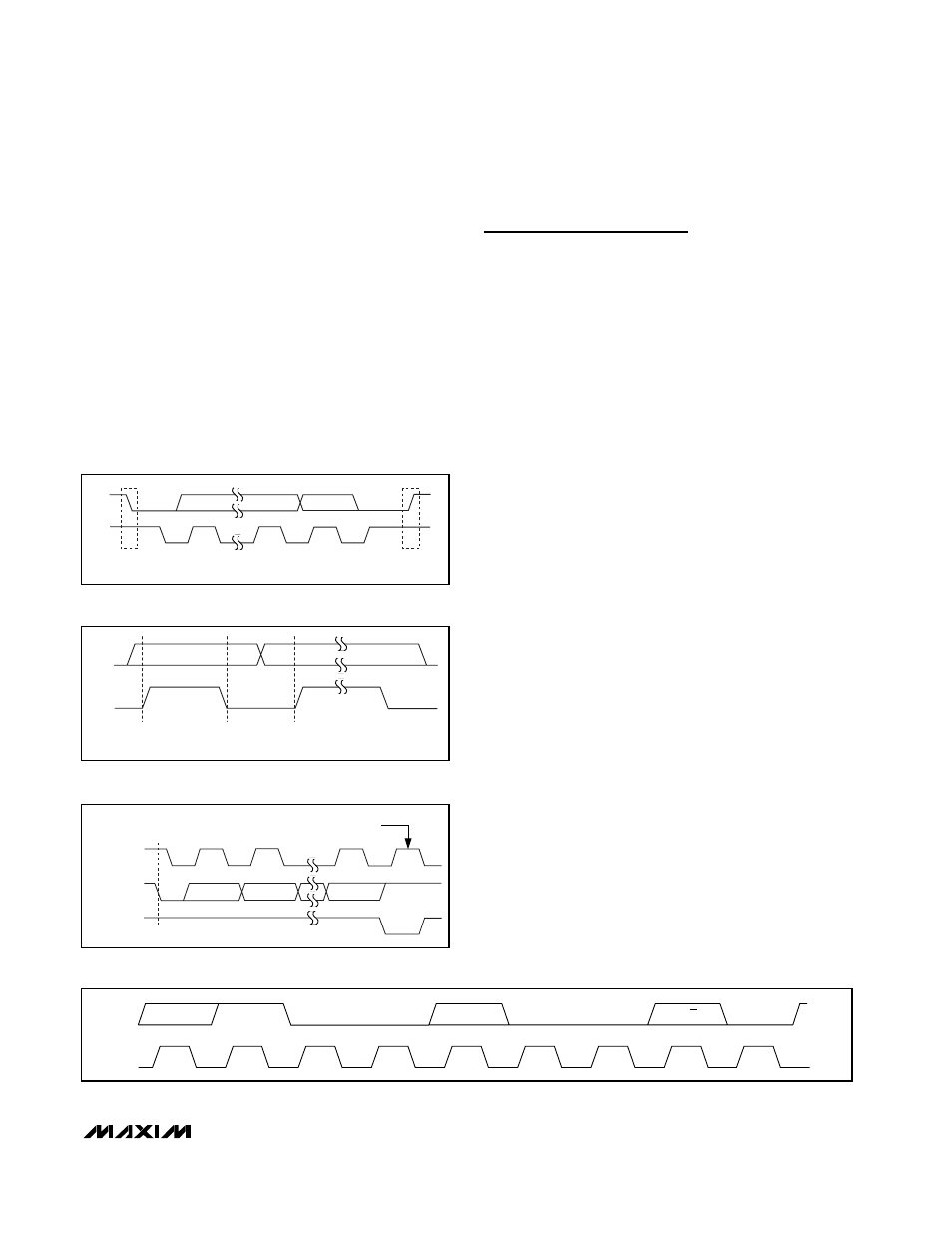
Each transmission consists of a START condition
(
Figure 3
) sent by a master, followed by the MAX6964
7-bit slave address plus R/W bit, a register address
byte, 1 or more data bytes, and finally a STOP condi-
tion (
Figure 3
).
Start and Stop Conditions
Both SCL and SDA remain high when the interface is
not busy. A master signals the beginning of a transmis-
sion with a START (S) condition by transitioning SDA
from high to low while SCL is high. When the master
has finished communicating with the slave, it issues a
STOP (P) condition by transitioning SDA from low to
high while SCL is high. The bus is then free for another
transmission (
Figure 3
).
Bit Transfer
One data bit is transferred during each clock pulse.
The data on SDA must remain stable while SCL is high
(
Figure 4
).
Acknowledge
The acknowledge bit is a clocked 9th bit that the recipi-
ent uses to handshake receipt of each byte of data
(
Figure 5
). Thus, each byte transferred effectively
requires 9 bits. The master generates the 9th clock
pulse, and the recipient pulls down SDA during the
acknowledge clock pulse so the SDA line is stable low
MAX6964
17-Output LED Driver/GPO
with Intensity Control
_______________________________________________________________________________________
7
Figure 3. Start and Stop Conditions
SDA
SCL
START
CONDITION
STOP
CONDITION
S
P
Figure 4. Bit Transfer
SDA
SCL
DATA LINE STABLE;
DATA VALID
CHANGE OF DATA
ALLOWED
Figure 5. Acknowledge
SCL
SDA BY
TRANSMITTER
CLOCK PULSE
FOR ACKNOWLEDGE
START
CONDITION
SDA BY
RECEIVER
1
2
8
9
S
Figure 6. Slave Address
SDA
SCL
1
MSB
LSB
ACK
0
0
A6
0
0
A2
R/W