Absolute maximum ratings, Recommended operating conditions, Dc electrical characteristics – Rainbow Electronics MAX34440 User Manual
Page 6
PMBus 6-Channel Power-Supply Manager
MAX34440
6
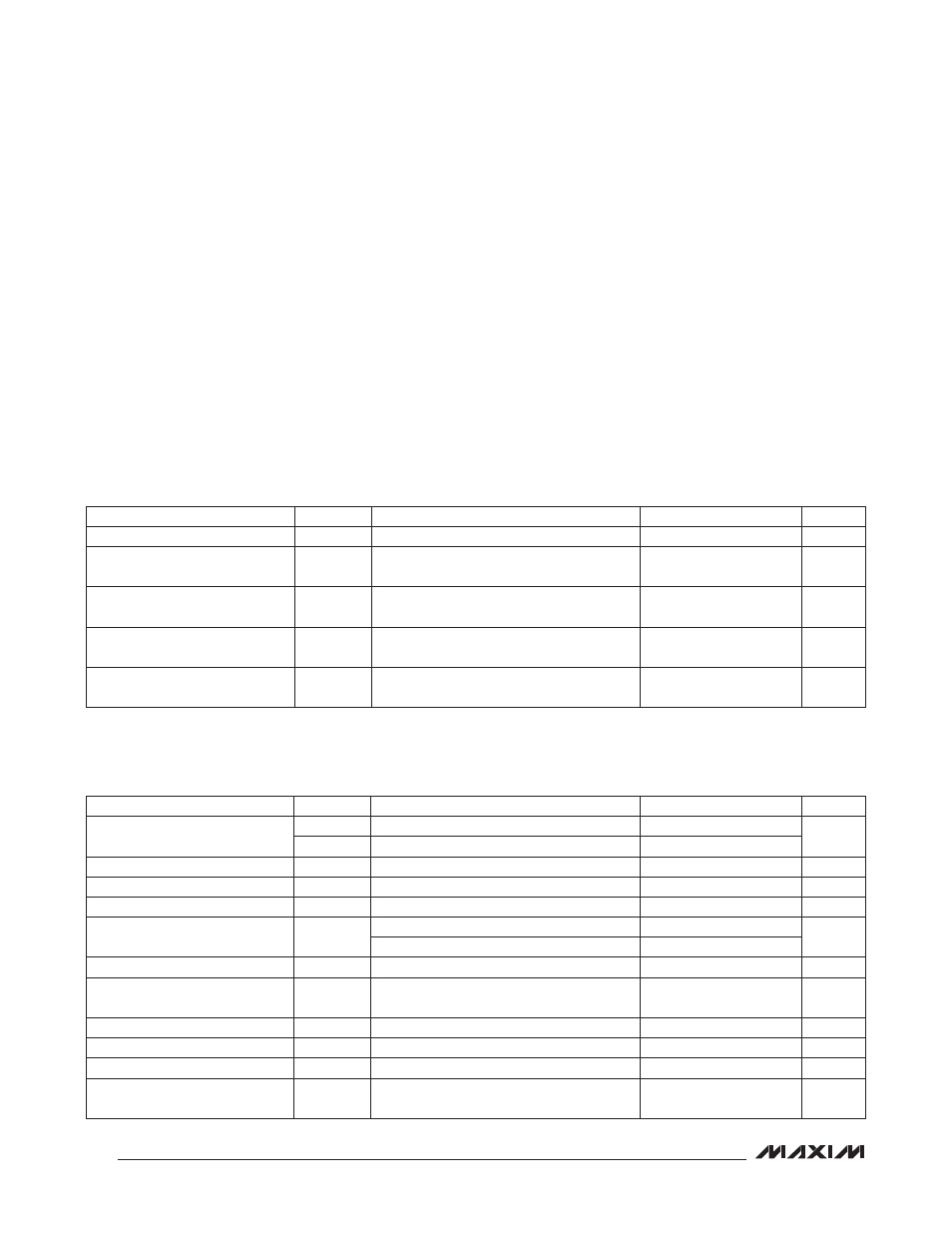
Stresses beyond those listed under “Absolute Maximum Ratings” may cause permanent damage to the device. These are stress ratings only, and functional
operation of the device at these or any other conditions beyond those indicated in the operational sections of the specifications is not implied. Exposure to absolute
maximum rating conditions for extended periods may affect device reliability.
V
DD
to V
SS
...........................................................-0.3V to +5.5V
RS- to V
SS
............................................................-0.3V to +0.3V
All Other Pins Except REG18 and
REG25 Relative to V
SS
........................ -0.3V to (V
DD
+ 0.3V)*
Continuous Power Dissipation (T
A
= +70NC)
40-Pin TQFN
(derate 35.7mW/NC above +70NC) .........................2857.1mW
Operating Temperature Range .......................... -40NC to +85NC
Storage Temperature Range ............................ -55NC to +125NC
Lead Temperature (soldering, 10s) ................................+260NC
Soldering Temperature (reflow) ......................................+260NC
RECOMMENDED OPERATING CONDITIONS
(T
A
= -40NC to +85NC.)
ABSOLUTE MAXIMUM RATINGS
DC ELECTRICAL CHARACTERISTICS
(V
DD
= 2.7V to 5.5V, T
A
= -40NC to +85NC, unless otherwise noted. Typical values are at V
DD
= 3.3V, T
A
= +25NC, unless otherwise noted.)
*Subject to not exceeding +5.5V.
PARAMETER
SYMBOL
CONDITIONS
MIN
TYP
MAX
UNITS
V
DD
Operating Voltage Range
V
DD
(Note 1)
2.7
5.5
V
Input Logic 1
V
IH
0.7 x
V
DD
V
DD
+
0.3
V
Input Logic 0
V
IL
-0.3
0.3 x
V
DD
V
Input Logic-High: SCL, SDA,
MSCL, MSDA
V
I2C_IH
2.7V P V
DD
P 3.6V (Note 1)
2.1
V
DD
+
0.3
V
Input Logic-Low: SCL, SDA,
MSCL, MSDA
V
I2C_IL
2.7V P V
DD
P 3.6V (Note 1)
-0.3
+0.8
V
PARAMETER
SYMBOL
CONDITIONS
MIN
TYP
MAX
UNITS
Supply Current
I
CPU
(Note 2)
2.5
mA
I
PROGRAM
8
Brownout Voltage
V
BO
Monitors V
DD
(Note 1)
2.40
2.46
2.55
V
Brownout Hysteresis
V
BOH
Monitors V
DD
(Note 1)
30
mV
Internal System Clock
f
MOSC
4.0
MHz
System Clock Error (Note 3)
f
ERR:MOSC
+25NC P T
A
P +85NC
-3
+2
%
-40NC P T
A
P +25NC
-6.5
+1.6
Output Logic-Low
V
OL1
I
OL
= 4mA (Note 1)
0.4
V
Output Logic-High
V
OH1
I
OH
= -2mA (Note 1)
V
DD
-
0.5
V
PWM, PSEN Pullup Current
I
PU
V
PIN
= V
SS
, V
DD
= 3.3V
38
55
107
F
A
ADC Internal Reference
1.225
V
ADC Voltage Measurement Error
V
ERR
-1
+1
%
ADC Internal Reference
Temperature Drift
-0.5
+0.5
%