Pin configuration, Pin description, Pin configuration pin description – Rainbow Electronics MAX34440 User Manual
Page 10: Pin description pin configuration
PMBus 6-Channel Power-Supply Manager
MAX34440
10
Pin Description
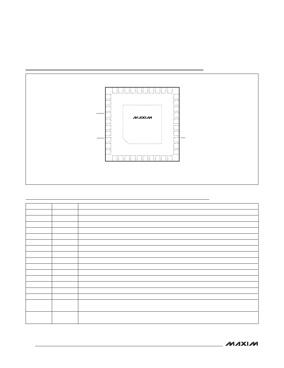
Pin Configuration
PIN
NAME
FUNCTION
1
RS-4
Ground Reference for ADC4 Voltage Measurement
2, 21, 36
V
SS
Digital-Supply Return Node (Ground)
3
RS+4
Power-Supply ADC Voltage-Sense Input, Measurement Relative to RS-4
4
RS-3
Ground Reference for ADC3 Voltage Measurement
5
RS+3
Power-Supply ADC Voltage-Sense Input, Measurement Relative to RS-3
6
RS+0
Power-Supply ADC Voltage-Sense Input, Measurement Relative to RS-0
7
RS-0
Ground Reference for ADC0 Voltage Measurement
8
RS+1
Power-Supply ADC Voltage-Sense Input, Measurement Relative to RS-1
9
V
DD
Supply Voltage. Bypass V
DD
to V
SS
with a 0.1FF capacitor.
10
RS-1
Ground Reference for ADC1 Voltage Measurement
11
RS+2
Power-Supply ADC Voltage-Sense Input, Measurement Relative to RS-2
12
RS-2
Ground Reference for ADC2 Voltage Measurement
13
RST
Reset Active-Low Input
14
MSDA
Master I
2
C Data Input/Output. Open-drain output.
15
MSCL
Master I
2
C Clock Output. Open-drain output.
16
PWM5
PWM Margin Output #5. High impedance when the margining is disabled. A 100% duty cycle implies
this pin is continuously high.
17
PSEN5
Power-Supply Enable Output #5. Programmable through MFR_MODE for either active high or active
low and either open drain or CMOS push-pull.
TOP VIEW
35
36
34
33
12
11
13
V
SS
RS-3
RS+3
RS+0
RS-0
14
RS-4
PSEN1
PSEN2
PWM2
PWM0
REG25
PSEN0
PSEN3
REG18
1
2
4
5
6
7
27
28
29
30
26
24 23 22
CONTROL
V
SS
PWM4
PSEN5
PWM5
MSCL
RS+4
PWM1
3
25
37
A1/PG
MSDA
38
39
40
RS-5
RS+5
RS-2
RS+2
EP
A0/MUXSEL
32
15
PSEN4
SCL
31
16
17
18
19
20 PWM3
RS+1
V
DD
RS-1
V
SS
8
9
10
21
SDA
FAULT
ALERT
RST
+
TQFN
(6mm × 6mm × 0.75mm)
MAX34440